AT90PWM2/3/2B/3B
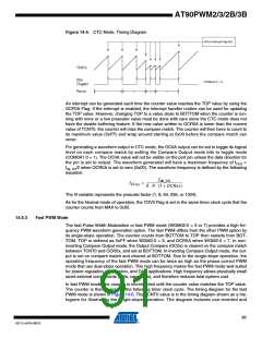
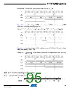
Figure 14-9. Timer/Counter Timing Diagram, with Prescaler (fclk_I/O/8)
clkI/O
clkTn
(clkI/O/8)
TCNTn
TOVn
MAX - 1
MAX
BOTTOM
BOTTOM + 1
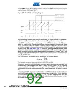
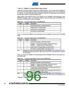
Figure 14-10 shows the setting of OCF0B in all modes and OCF0A in all modes except CTC
mode and PWM mode, where OCR0A is TOP.
Figure 14-10. Timer/Counter Timing Diagram, Setting of OCF0x, with Prescaler (fclk_I/O/8)
clkI/O
clkTn
(clkI/O/8)
TCNTn
OCRnx
OCFnx
OCRnx - 1
OCRnx
OCRnx + 1
OCRnx + 2
OCRnx Value
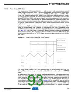
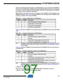
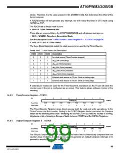
Figure 14-11 shows the setting of OCF0A and the clearing of TCNT0 in CTC mode and fast
PWM mode where OCR0A is TOP.
Figure 14-11. Timer/Counter Timing Diagram, Clear Timer on Compare Match mode, with Pres-
caler (fclk_I/O/8)
clkI/O
clkTn
(clkI/O/8)
TCNTn
(CTC)
TOP - 1
TOP
BOTTOM
BOTTOM + 1
OCRnx
TOP
OCFnx
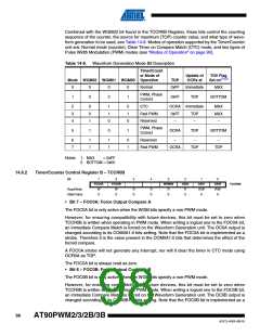
14.8 8-bit Timer/Counter Register Description
14.8.1
Timer/Counter Control Register A – TCCR0A
Bit
7
COM0A1
R/W
6
COM0A0
R/W
5
COM0B1
R/W
4
COM0B0
R/W
3
2
–
1
WGM01
R/W
0
0
WGM00
R/W
0
–
R
0
TCCR0A
Read/Write
Initial Value
R
0
0
0
0
0
95
4317J–AVR–08/10

 ATMEL [ ATMEL ]