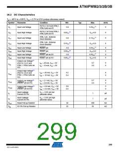
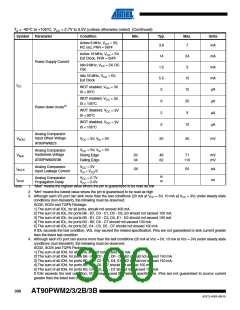
TA = -40°C to +105°C, VCC = 2.7V to 5.5V (unless otherwise noted) (Continued)
Symbol
Parameter
Condition
Min.
Typ.
Max.
Units
Active 8 MHz, VCC = 3V,
RC osc, PRR = 0xFF
3.8
7
mA
Active 16 MHz, VCC = 5V,
Ext Clock, PRR = 0xFF
14
1.5
5.5
5
24
3
mA
mA
mA
µA
Power Supply Current
Idle 8 MHz, VCC = 3V, RC
Osc
Idle 16 MHz, VCC = 5V,
Ext Clock
10
15
ICC
WDT enabled, VCC = 3V
t0 < 90°C
WDT enabled, VCC = 3V
t0 < 105°C
9
2
5
20
3
µA
µA
µA
Power-down mode(5)
WDT disabled, VCC = 3V
t0 < 90°C
WDT disabled, VCC = 3V
t0 < 105°C
10
Analog Comparator
Input Offset Voltage
VACIO
VCC = 5V, Vin = 3V
20
50
mV
AT90PWM2/3
VCC = 5V, Vin = 3V
Rising Edge
Analog Comparator
Hysteresis Voltage
Vhysr
33
34
46
62
71
mV
mV
AT90PWM2B/3B
Falling Edge
110
Analog Comparator
Input Leakage Current
VCC = 5V
Vin = VCC/2
IACLK
tACID
-50
50
nA
ns
(6)
(6)
Analog Comparator
Propagation Delay
VCC = 2.7V
VCC = 5.0V
Note:
1. “Max” means the highest value where the pin is guaranteed to be read as low
2. “Min” means the lowest value where the pin is guaranteed to be read as high
3. Although each I/O port can sink more than the test conditions (20 mA at VCC = 5V, 10 mA at VCC = 3V) under steady state
conditions (non-transient), the following must be observed:
SO32, SO24 and TQFN Package:
1] The sum of all IOL, for all ports, should not exceed 400 mA.
2] The sum of all IOL, for ports B6 - B7, C0 - C1, D0 - D3, E0 should not exceed 100 mA.
3] The sum of all IOL, for ports B0 - B1, C2 - C3, D4, E1 - E2 should not exceed 100 mA.
4] The sum of all IOL, for ports B3 - B5, C6 - C7 should not exceed 100 mA.
5] The sum of all IOL, for ports B2, C4 - C5, D5 - D7 should not exceed 100 mA.
If IOL exceeds the test condition, VOL may exceed the related specification. Pins are not guaranteed to sink current greater
than the listed test condition.
4. Although each I/O port can source more than the test conditions (20 mA at Vcc = 5V, 10 mA at Vcc = 3V) under steady state
conditions (non-transient), the following must be observed:
SO32, SO24 and TQFN Package:
1] The sum of all IOH, for all ports, should not exceed 400 mA.
2] The sum of all IOH, for ports B6 - B7, C0 - C1, D0 - D3, E0 should not exceed 150 mA.
3] The sum of all IOH, for ports B0 - B1, C2 - C3, D4, E1 - E2 should not exceed 150 mA.
4] The sum of all IOH, for ports B3 - B5, C6 - C7 should not exceed 150 mA.
5] The sum of all IOH, for ports B2, C4 - C5, D5 - D7 should not exceed 150 mA.
If IOH exceeds the test condition, VOH may exceed the related specification. Pins are not guaranteed to source current
greater than the listed test condition.
300
AT90PWM2/3/2B/3B
4317J–AVR–08/10

 ATMEL [ ATMEL ]