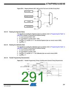
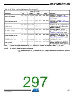
AT90PWM2/3/2B/3B
Memory Page instruction. To ensure correct loading of the page, the data low byte must
be loaded before data high byte is applied for a given address. The Program Memory
Page is stored by loading the Write Program Memory Page instruction with the 8 MSB of
the address. If polling is not used, the user must wait at least tWD_FLASH before issuing the
next page. (See Table 25-15.) Accessing the serial programming interface before the
Flash write operation completes can result in incorrect programming.
5. The EEPROM array is programmed one byte at a time by supplying the address and data
together with the appropriate Write instruction. An EEPROM memory location is first
automatically erased before new data is written. If polling is not used, the user must wait
at least tWD_EEPROM before issuing the next byte. (See Table 25-15.) In a chip erased
device, no 0xFFs in the data file(s) need to be programmed.
6. Any memory location can be verified by using the Read instruction which returns the con-
tent at the selected address at serial output MISO.
7. At the end of the programming session, RESET can be set high to commence normal
operation.
8. Power-off sequence (if needed):
Set RESET to “1”.
Turn VCC power off.
25.9.2
Data Polling Flash
When a page is being programmed into the Flash, reading an address location within the page
being programmed will give the value 0xFF. At the time the device is ready for a new page, the
programmed value will read correctly. This is used to determine when the next page can be writ-
ten. Note that the entire page is written simultaneously and any address within the page can be
used for polling. Data polling of the Flash will not work for the value 0xFF, so when programming
this value, the user will have to wait for at least tWD_FLASH before programming the next page. As
a chip-erased device contains 0xFF in all locations, programming of addresses that are meant to
contain 0xFF, can be skipped. See Table 25-15 for tWD_FLASH value.
25.9.3
Data Polling EEPROM
When a new byte has been written and is being programmed into EEPROM, reading the
address location being programmed will give the value 0xFF. At the time the device is ready for
a new byte, the programmed value will read correctly. This is used to determine when the next
byte can be written. This will not work for the value 0xFF, but the user should have the following
in mind: As a chip-erased device contains 0xFF in all locations, programming of addresses that
are meant to contain 0xFF, can be skipped. This does not apply if the EEPROM is re-pro-
grammed without chip erasing the device. In this case, data polling cannot be used for the value
0xFF, and the user will have to wait at least tWD_EEPROM before programming the next byte. See
Table 25-15 for tWD_EEPROM value.
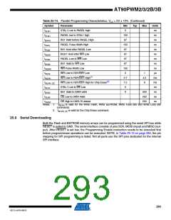
Table 25-15. Minimum Wait Delay Before Writing the Next Flash or EEPROM Location
Symbol
Minimum Wait Delay
4.5 ms
tWD_FLASH
tWD_EEPROM
tWD_ERASE
3.6 ms
9.0 ms
295
4317J–AVR–08/10

 ATMEL [ ATMEL ]