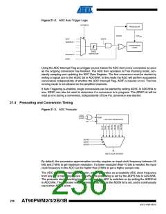
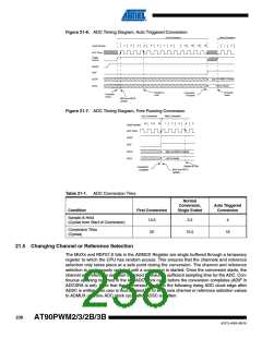
Figure 21-6. ADC Timing Diagram, Auto Triggered Conversion
One Conversion
Next Conversion
1
2
3
4
5
6
7
8
13
14
15
16
1
2
Cycle Number
ADC Clock
Trigger
Source
ADATE
ADIF
ADCH
ADCL
Sign and MSB of Result
LSB of Result
Sample &
Hold
Prescaler
Reset
Conversion
Complete
Prescaler
Reset
MUX and REFS
Update
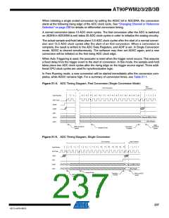
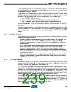
Figure 21-7. ADC Timing Diagram, Free Running Conversion
One Conversion
Next Conversion
14
15
16
1
2
3
4
5
Cycle Number
ADC Clock
ADSC
ADIF
ADCH
ADCL
Sign and MSB of Result
LSB of Result
Sample & Hold
MUX and REFS
Update
Conversion
Complete
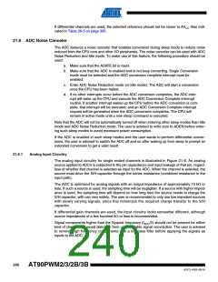
Table 21-1. ADC Conversion Time
Normal
Conversion,
Single Ended
Auto Triggered
Conversion
Condition
First Conversion
Sample & Hold
(Cycles from Start of Conversion)
13.5
3.5
4
Conversion Time
(Cycles)
25
15.5
16
21.5 Changing Channel or Reference Selection
The MUXn and REFS1:0 bits in the ADMUX Register are single buffered through a temporary
register to which the CPU has random access. This ensures that the channels and reference
selection only takes place at a safe point during the conversion. The channel and reference
selection is continuously updated until a conversion is started. Once the conversion starts, the
channel and reference selection is locked to ensure a sufficient sampling time for the ADC. Con-
tinuous updating resumes in the last ADC clock cycle before the conversion completes (ADIF in
ADCSRA is set). Note that the conversion starts on the following rising ADC clock edge after
ADSC is written. The user is thus advised not to write new channel or reference selection values
to ADMUX until one ADC clock cycle after ADSC is written.
238
AT90PWM2/3/2B/3B
4317J–AVR–08/10

 ATMEL [ ATMEL ]