AT90PWM2/3/2B/3B
The PWM frequency for the output can be calculated by the following equation:
f
clk_I/O
f
= ----------------------------------
OCnxPWM
N ⋅ (1 + TOP)
The N variable represents the prescaler divider (1, 8, 64, 256, or 1024).
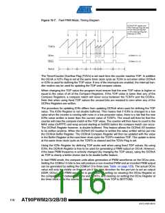
The extreme values for the OCRnx Register represents special cases when generating a PWM
waveform output in the fast PWM mode. If the OCRnx is set equal to BOTTOM (0x0000) the out-
put will be a narrow spike for each TOP+1 timer clock cycle. Setting the OCRnx equal to TOP
will result in a constant high or low output (depending on the polarity of the output set by the
COMnx1:0 bits.)
A frequency (with 50% duty cycle) waveform output in fast PWM mode can be achieved by set-
ting OCnA to toggle its logical level on each compare match (COMnA1:0 = 1). This applies only
if OCR1A is used to define the TOP value (WGM13:0 = 15). The waveform generated will have
a maximum frequency of fOC A = fclk_I/O/2 when OCRnA is set to zero (0x0000). This feature is
n
similar to the OCnA toggle in CTC mode, except the double buffer feature of the Output Com-
pare unit is enabled in the fast PWM mode.
15.8.4
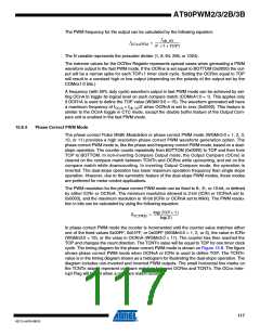
Phase Correct PWM Mode
The phase correct Pulse Width Modulation or phase correct PWM mode (WGMn3:0 = 1, 2, 3,
10, or 11) provides a high resolution phase correct PWM waveform generation option. The
phase correct PWM mode is, like the phase and frequency correct PWM mode, based on a dual-
slope operation. The counter counts repeatedly from BOTTOM (0x0000) to TOP and then from
TOP to BOTTOM. In non-inverting Compare Output mode, the Output Compare (OCnx) is
cleared on the compare match between TCNTn and OCRnx while upcounting, and set on the
compare match while downcounting. In inverting Output Compare mode, the operation is
inverted. The dual-slope operation has lower maximum operation frequency than single slope
operation. However, due to the symmetric feature of the dual-slope PWM modes, these modes
are preferred for motor control applications.
The PWM resolution for the phase correct PWM mode can be fixed to 8-, 9-, or 10-bit, or defined
by either ICRn or OCRnA. The minimum resolution allowed is 2-bit (ICRn or OCRnA set to
0x0003), and the maximum resolution is 16-bit (ICRn or OCRnA set to MAX). The PWM resolu-
tion in bits can be calculated by using the following equation:
log(TOP + 1)
R
= ----------------------------------
PCPWM
log(2)
In phase correct PWM mode the counter is incremented until the counter value matches either
one of the fixed values 0x00FF, 0x01FF, or 0x03FF (WGMn3:0 = 1, 2, or 3), the value in ICRn
(WGMn3:0 = 10), or the value in OCRnA (WGMn3:0 = 11). The counter has then reached the
TOP and changes the count direction. The TCNTn value will be equal to TOP for one timer clock
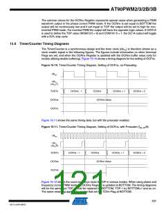
cycle. The timing diagram for the phase correct PWM mode is shown on Figure 15-8. The figure
shows phase correct PWM mode when OCRnA or ICRn is used to define TOP. The TCNTn
value is in the timing diagram shown as a histogram for illustrating the dual-slope operation. The
diagram includes non-inverted and inverted PWM outputs. The small horizontal line marks on
the TCNTn slopes represent compare matches between OCRnx and TCNTn. The OCnx Inter-
rupt Flag will be set when a compare match occurs.
117
4317J–AVR–08/10

 ATMEL [ ATMEL ]