updated by the value written. Then when the low byte (OCRnxL) is written to the lower eight bits,
the high byte will be copied into the upper 8-bits of either the OCRnx buffer or OCRnx Compare
Register in the same system clock cycle.
For more information of how to access the 16-bit registers refer to “Accessing 16-bit Registers”
on page 104.
15.6.1
Force Output Compare
In non-PWM Waveform Generation modes, the match output of the comparator can be forced by
writing a one to the Force Output Compare (FOCnx) bit. Forcing compare match will not set the
OCFnx Flag or reload/clear the timer, but the OCnx pin will be updated as if a real compare
match had occurred (the COMn1:0 bits settings define whether the OCnx pin is set, cleared or
toggled).
15.6.2
15.6.3
Compare Match Blocking by TCNTn Write
All CPU writes to the TCNTn Register will block any compare match that occurs in the next timer
clock cycle, even when the timer is stopped. This feature allows OCRnx to be initialized to the
same value as TCNTn without triggering an interrupt when the Timer/Counter clock is enabled.
Using the Output Compare Unit
Since writing TCNTn in any mode of operation will block all compare matches for one timer clock
cycle, there are risks involved when changing TCNTn when using any of the Output Compare
channels, independent of whether the Timer/Counter is running or not. If the value written to
TCNTn equals the OCRnx value, the compare match will be missed, resulting in incorrect wave-
form generation. Do not write the TCNTn equal to TOP in PWM modes with variable TOP
values. The compare match for the TOP will be ignored and the counter will continue to 0xFFFF.
Similarly, do not write the TCNTn value equal to BOTTOM when the counter is downcounting.
The setup of the OCnx should be performed before setting the Data Direction Register for the
port pin to output. The easiest way of setting the OCnx value is to use the Force Output Com-
pare (FOCnx) strobe bits in Normal mode. The OCnx Register keeps its value even when
changing between Waveform Generation modes.
Be aware that the COMnx1:0 bits are not double buffered together with the compare value.
Changing the COMnx1:0 bits will take effect immediately.
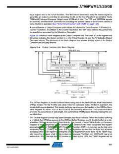
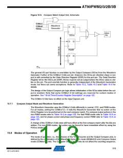
15.7 Compare Match Output Unit
The Compare Output mode (COMnx1:0) bits have two functions. The Waveform Generator uses
the COMnx1:0 bits for defining the Output Compare (OCnx) state at the next compare match.
Secondly the COMnx1:0 bits control the OCnx pin output source. Figure 15-5 shows a simplified
schematic of the logic affected by the COMnx1:0 bit setting. The I/O Registers, I/O bits, and I/O
pins in the figure are shown in bold. Only the parts of the general I/O Port Control Registers
(DDR and PORT) that are affected by the COMnx1:0 bits are shown. When referring to the
OCnx state, the reference is for the internal OCnx Register, not the OCnx pin. If a system reset
occur, the OCnx Register is reset to “0”.
112
AT90PWM2/3/2B/3B
4317J–AVR–08/10

 ATMEL [ ATMEL ]