AT90PWM2/3/2B/3B
ing a logical one to its I/O bit location. The Waveform Generator uses the match signal to
generate an output according to operating mode set by the Waveform Generation mode
(WGMn3:0) bits and Compare Output mode (COMnx1:0) bits. The TOP and BOTTOM signals
are used by the Waveform Generator for handling the special cases of the extreme values in
some modes of operation (See “16-bit Timer/Counter1 with PWM” on page 102.)
A special feature of Output Compare unit A allows it to define the Timer/Counter TOP value (i.e.,
counter resolution). In addition to the counter resolution, the TOP value defines the period time
for waveforms generated by the Waveform Generator.
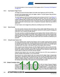
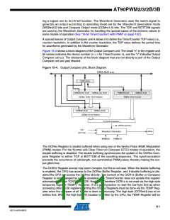
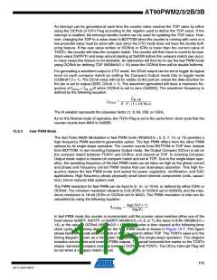
Figure 15-4 shows a block diagram of the Output Compare unit. The small “n” in the register and
bit names indicates the device number (n = n for Timer/Counter n), and the “x” indicates Output
Compare unit (x). The elements of the block diagram that are not directly a part of the Output
Compare unit are gray shaded.
Figure 15-4. Output Compare Unit, Block Diagram
DATA BUS (8-bit)
TEMP (8-bit)
OCRnxH Buf. (8-bit)
OCRnxL Buf. (8-bit)
TCNTnH (8-bit)
TCNTnL (8-bit)
OCRnx Buffer (16-bit Register)
TCNTn (16-bit Counter)
OCRnxH (8-bit)
OCRnxL (8-bit)
OCRnx (16-bit Register)
=
(16-bit Comparator )
OCFnx (Int.Req.)
TOP
OCnx
Waveform Generator
BOTTOM
WGMn3:0
COMnx1:0
The OCRnx Register is double buffered when using any of the twelve Pulse Width Modulation
(PWM) modes. For the Normal and Clear Timer on Compare (CTC) modes of operation, the
double buffering is disabled. The double buffering synchronizes the update of the OCRnx Com-
pare Register to either TOP or BOTTOM of the counting sequence. The synchronization
prevents the occurrence of odd-length, non-symmetrical PWM pulses, thereby making the out-
put glitch-free.
The OCRnx Register access may seem complex, but this is not case. When the double buffering
is enabled, the CPU has access to the OCRnx Buffer Register, and if double buffering is dis-
abled the CPU will access the OCRnx directly. The content of the OCR1x (Buffer or Compare)
Register is only changed by a write operation (the Timer/Counter does not update this register
automatically as the TCNT1 and ICR1 Register). Therefore OCR1x is not read via the high byte
temporary register (TEMP). However, it is a good practice to read the low byte first as when
accessing other 16-bit registers. Writing the OCRnx Registers must be done via the TEMP Reg-
ister since the compare of all 16 bits is done continuously. The high byte (OCRnxH) has to be
written first. When the high byte I/O location is written by the CPU, the TEMP Register will be
111
4317J–AVR–08/10

 ATMEL [ ATMEL ]