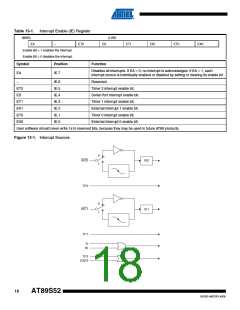
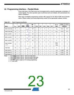
19. Programming the Flash – Serial Mode
The Code memory array can be programmed using the serial ISP interface while RST is pulled
to VCC. The serial interface consists of pins SCK, MOSI (input) and MISO (output). After RST is
set high, the Programming Enable instruction needs to be executed first before other operations
can be executed. Before a reprogramming sequence can occur, a Chip Erase operation is
required.
The Chip Erase operation turns the content of every memory location in the Code array into
FFH.
Either an external system clock can be supplied at pin XTAL1 or a crystal needs to be connected
across pins XTAL1 and XTAL2. The maximum serial clock (SCK) frequency should be less than
1/16 of the crystal frequency. With a 33 MHz oscillator clock, the maximum SCK frequency is
2 MHz.
20. Serial Programming Algorithm
To program and verify the AT89S52 in the serial programming mode, the following sequence is
recommended:
1. Power-up sequence:
a. Apply power between VCC and GND pins.
b. Set RST pin to “H”.
If a crystal is not connected across pins XTAL1 and XTAL2, apply a 3 MHz to 33 MHz clock to
XTAL1 pin and wait for at least 10 milliseconds.
2. Enable serial programming by sending the Programming Enable serial instruction to pin
MOSI/P1.5. The frequency of the shift clock supplied at pin SCK/P1.7 needs to be less
than the CPU clock at XTAL1 divided by 16.
3. The Code array is programmed one byte at a time in either the Byte or Page mode. The
write cycle is self-timed and typically takes less than 0.5 ms at 5V.
4. Any memory location can be verified by using the Read instruction which returns the
content at the selected address at serial output MISO/P1.6.
5. At the end of a programming session, RST can be set low to commence normal device
operation.
Power-off sequence (if needed):
1. Set XTAL1 to “L” (if a crystal is not used).
2. Set RST to “L”.
3. Turn VCC power off.
Data Polling: The Data Polling feature is also available in the serial mode. In this mode, during
a write cycle an attempted read of the last byte written will result in the complement of the MSB
of the serial output byte on MISO.
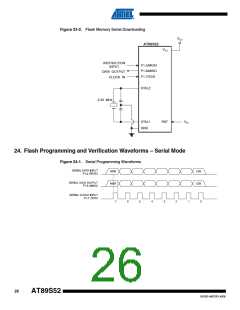
21. Serial Programming Instruction Set
The Instruction Set for Serial Programming follows a 4-byte protocol and is shown in Table 24-1.
22
AT89S52
1919D–MICRO–6/08

 ATMEL [ ATMEL ]