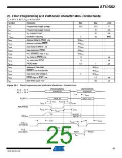
AT89S52
18. Programming the Flash – Parallel Mode
The AT89S52 is shipped with the on-chip Flash memory array ready to be programmed. The
programming interface needs a high-voltage (12-volt) program enable signal and is compatible
with conventional third-party Flash or EPROM programmers.
The AT89S52 code memory array is programmed byte-by-byte.
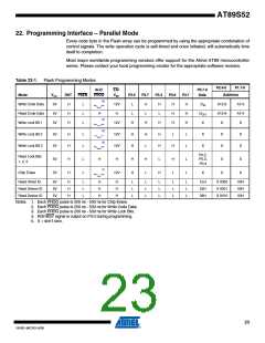
Programming Algorithm: Before programming the AT89S52, the address, data, and control
signals should be set up according to the “Flash Programming Modes” (Table 22-1) and Figure
22-1 and Figure 22-2. To program the AT89S52, take the following steps:
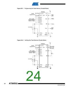
1. Input the desired memory location on the address lines.
2. Input the appropriate data byte on the data lines.
3. Activate the correct combination of control signals.
4. Raise EA/VPP to 12V.
5. Pulse ALE/PROG once to program a byte in the Flash array or the lock bits. The byte-
write cycle is self-timed and typically takes no more than 50 µs. Repeat steps 1
through 5, changing the address and data for the entire array or until the end of the
object file is reached.
Data Polling: The AT89S52 features Data Polling to indicate the end of a byte write cycle. Dur-
ing a write cycle, an attempted read of the last byte written will result in the complement of the
written data on P0.7. Once the write cycle has been completed, true data is valid on all outputs,
and the next cycle may begin. Data Polling may begin any time after a write cycle has been
initiated.
Ready/Busy: The progress of byte programming can also be monitored by the RDY/BSY output
signal. P3.0 is pulled low after ALE goes high during programming to indicate BUSY. P3.0 is
pulled high again when programming is done to indicate READY.
Program Verify: If lock bits LB1 and LB2 have not been programmed, the programmed code
data can be read back via the address and data lines for verification. The status of the individ-
ual lock bits can be verified directly by reading them back.
Reading the Signature Bytes: The signature bytes are read by the same procedure as a nor-
mal verification of locations 000H, 100H, and 200H, except that P3.6 and P3.7 must be pulled to
a logic low. The values returned are as follows.
(000H) = 1EH indicates manufactured by Atmel
(100H) = 52H indicates AT89S52
(200H) = 06H
Chip Erase: In the parallel programming mode, a chip erase operation is initiated by using the
proper combination of control signals and by pulsing ALE/PROG low for a duration of 200 ns -
500 ns.
In the serial programming mode, a chip erase operation is initiated by issuing the Chip Erase
instruction. In this mode, chip erase is self-timed and takes about 500 ms.
During chip erase, a serial read from any address location will return 00H at the data output.
21
1919D–MICRO–6/08

 ATMEL [ ATMEL ]