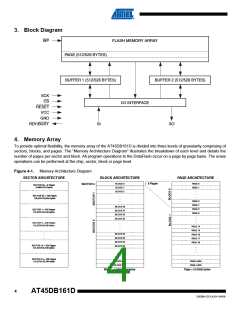
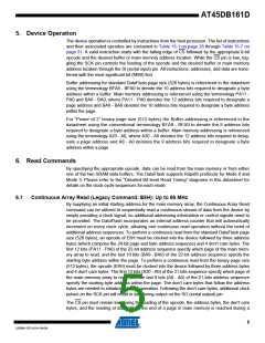
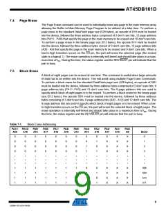
3. Block Diagram
WP
FLASH MEMORY ARRAY
PAGE (512/528 BYTES)
BUFFER 1 (512/528 BYTES)
BUFFER 2 (512/528 BYTES)
SCK
CS
I/O INTERFACE
RESET
VCC
GND
RDY/BUSY
SI
SO
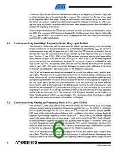
4. Memory Array
To provide optimal flexibility, the memory array of the AT45DB161D is divided into three levels of granularity comprising of
sectors, blocks, and pages. The “Memory Architecture Diagram” illustrates the breakdown of each level and details the
number of pages per sector and block. All program operations to the DataFlash occur on a page by page basis. The erase
operations can be performed at the chip, sector, block or page level.
Figure 4-1. Memory Architecture Diagram
SECTOR ARCHITECTURE
BLOCK ARCHITECTURE
PAGE ARCHITECTURE
BLOCK 0
BLOCK 1
BLOCK 2
8 Pages
PAGE 0
PAGE 1
SECTOR 0
SECTOR 0a = 8 Pages
4,096/4,224 bytes
SECTOR 0b = 248 Pages
126,976/130,944 bytes
PAGE 6
PAGE 7
PAGE 8
PAGE 9
BLOCK 30
BLOCK 31
BLOCK 32
BLOCK 33
SECTOR 1 = 256 Pages
131,072/135,168 bytes
SECTOR 2 = 256 Pages
131,072/135,168 bytes
PAGE 14
PAGE 15
PAGE 16
PAGE 17
PAGE 18
BLOCK 62
BLOCK 63
BLOCK 64
BLOCK 65
SECTOR 14 = 256 Pages
131,072/135,168 bytes
SECTOR 15 = 256 Pages
131,072/135,168 bytes
BLOCK 510
BLOCK 511
PAGE 4,094
PAGE 4,095
Block = 4,096/4,224 bytes
Page = 512/528 bytes
4
AT45DB161D
3500M–DFLASH–04/09

 ATMEL [ ATMEL ]