address lines and a parallel interface, the DataFlash uses a RapidS serial interface to sequen-
tially access its data. The simple sequential access dramatically reduces active pin count,
facilitates hardware layout, increases system reliability, minimizes switching noise, and reduces
package size. The device is optimized for use in many commercial and industrial applications
where high-density, low-pin count, low-voltage and low-power are essential.
To allow for simple in-system reprogrammability, the AT45DB161D does not require high input
voltages for programming. The device operates from a single power supply, 2.5V to 3.6V or 2.7V
to 3.6V, for both the program and read operations. The AT45DB161D is enabled through the
chip select pin (CS) and accessed via a three-wire interface consisting of the Serial Input (SI),
Serial Output (SO), and the Serial Clock (SCK).
All programming and erase cycles are self-timed.
2. Pin Configurations and Pinouts
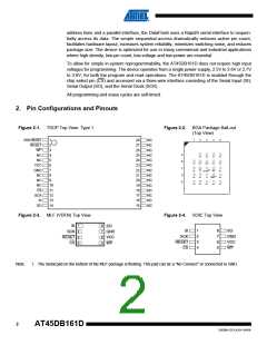
Figure 2-1. TSOP Top View: Type 1
Figure 2-2. BGA Package Ball-out
(Top View)
1
2
3
4
5
RDY/BUSY
RESET
WP
1
28
27
26
25
24
23
22
21
20
19
18
17
16
15
NC
NC
NC
NC
NC
NC
NC
NC
NC
NC
NC
NC
NC
NC
2
3
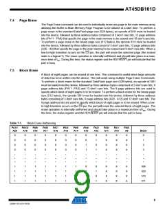
A
B
C
D
E
NC
4
NC
NC
NC
NC
NC
NC
5
NC
SCK
GND
VCC
VCC
GND
NC
6
7
NC
NC
NC
CS RDY/BSY
WP
RESET
NC
NC
NC
NC
8
SO
NC
SI
NC
9
NC
NC
10
11
12
13
14
CS
SCK
SI
SO
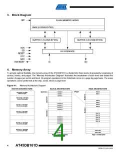
Figure 2-3. MLF (VDFN) Top View
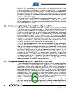
Figure 2-4. SOIC Top View
SI
SCK
1
2
3
4
8
7
6
5
SO
SI
SCK
1
2
3
4
8
7
6
5
SO
GND
VCC
WP
GND
VCC
WP
RESET
CS
RESET
CS
Note:
1. The metal pad on the bottom of the MLF package is floating. This pad can be a “No Connect” or connected to GND.
2
AT45DB161D
3500M–DFLASH–04/09

 ATMEL [ ATMEL ]