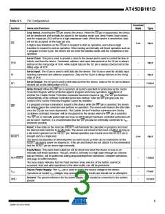
AT45DB161D
during the page boundary crossover (the crossover from the end of one page to the beginning of
the next page). When the last bit in the main memory array has been read, the device will con-
tinue reading back at the beginning of the first page of memory. As with crossing over page
boundaries, no delays will be incurred when wrapping around from the end of the array to the
beginning of the array. A low-to-high transition on the CS pin will terminate the read operation
and tri-state the output pin (SO). The Continuous Array Read bypasses both data buffers and
leaves the contents of the buffers unchanged.
6.4
Main Memory Page Read
A main memory page read allows the user to read data directly from any one of the 4,096 pages
in the main memory, bypassing both of the data buffers and leaving the contents of the buffers
unchanged. To start a page read from the standard DataFlash page size (528 bytes), an opcode
of D2H must be clocked into the device followed by three address bytes (which comprise the 24-
bit page and byte address sequence) and 4 don’t care bytes. The first 12 bits (PA11 - PA0) of
the 22-bit address sequence specify the page in main memory to be read, and the last 10 bits
(BA9 - BA0) of the 22-bit address sequence specify the starting byte address within that page.
To start a page read from the binary page size (512 bytes), the opcode D2H must be clocked
into the device followed by three address bytes and 4 don’t care bytes. The first 12 bits (A20 -
A9) of the 21-bits sequence specify which page of the main memory array to read, and the last 9
bits (A8 - A0) of the 21-bits address sequence specify the starting byte address within the page.
The don’t care bytes that follow the address bytes are sent to initialize the read operation. Fol-
lowing the don’t care bytes, additional pulses on SCK result in data being output on the SO
(serial output) pin. The CS pin must remain low during the loading of the opcode, the address
bytes, the don’t care bytes, and the reading of data. When the end of a page in main memory is
reached, the device will continue reading back at the beginning of the same page. A low-to-high
transition on the CS pin will terminate the read operation and tri-state the output pin (SO). The
maximum SCK frequency allowable for the Main Memory Page Read is defined by the fSCK
specification. The Main Memory Page Read bypasses both data buffers and leaves the contents
of the buffers unchanged.
6.5
Buffer Read
The SRAM data buffers can be accessed independently from the main memory array, and utiliz-
ing the Buffer Read Command allows data to be sequentially read directly from the buffers. Four
opcodes, D4H or D1H for buffer 1 and D6H or D3H for buffer 2 can be used for the Buffer Read
Command. The use of each opcode depends on the maximum SCK frequency that will be used
to read data from the buffer. The D4H and D6H opcode can be used at any SCK frequency up to
the maximum specified by fCAR1. The D1H and D3H opcode can be used for lower frequency
read operations up to the maximum specified by fCAR2
.
To perform a buffer read from the standard DataFlash buffer (528 bytes), the opcode must be
clocked into the device followed by three address bytes comprised of 14 don’t care bits and 10
buffer address bits (BFA9 - BFA0). To perform a buffer read from the binary buffer (512 bytes),
the opcode must be clocked into the device followed by three address bytes comprised of 15
don’t care bits and 9 buffer address bits (BFA8 - BFA0). Following the address bytes, one don’t
care byte must be clocked in to initialize the read operation. The CS pin must remain low during
the loading of the opcode, the address bytes, the don’t care bytes, and the reading of data.
When the end of a buffer is reached, the device will continue reading back at the beginning of
the buffer. A low-to-high transition on the CS pin will terminate the read operation and tri-state
the output pin (SO).
7
3500M–DFLASH–04/09

 ATMEL [ ATMEL ]