1.
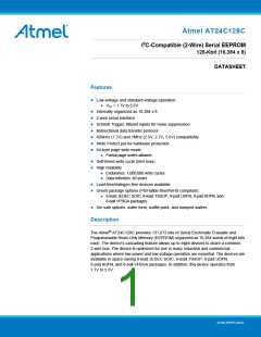
Pin Configurations and Pinouts
Table 1-1. Pin Configuration
8-lead SOIC
8-lead TSSOP
Pin
A0
Function
A0
A1
VCC
WP
1
2
3
4
8
7
6
5
1
2
3
4
8
7
6
5
A0
A1
VCC
WP
SCL
SDA
Address Input
Address Input
Address Input
Ground
A2
A2
SCL
SDA
A1
GND
GND
A2
Top View
Top View
GND
SDA
SCL
WP
VCC
Serial Data
8-pad UDFN/XDFN
8-ball VFBGA
Serial Clock Input
Write Protect
Device Power Supply
8
7
6
5
1
2
3
4
VCC
WP
A0
A0
A1
A2
1
2
3
4
8
7
6
5
VCC
WP
SCL
SDA
A1
SCL
SDA
A2
GND
GND
Top View
Bottom View
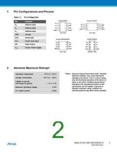
2.
Absolute Maximum Ratings*
*Notice: Stresses beyond those listed under “Absolute
Maximum Ratings” may cause permanent
damage to the device. This is a stress rating
only and functional operation of the device at
these or any other conditions beyond those
indicated in the operational sections of this
specification are not implied. Exposure to
absolute maximum rating conditions for
Operating Temperature . . . . . . . . . . .−55°C to +125°C
Storage Temperature . . . . . . . . . . . −65°C to + 150°C
Voltage on any pin
with respect to ground . . . . . . . . . . . . . . − 1.0 V +7.0V
Maximum Operating Voltage. . . . . . . . . . . . . . . 6.25V
DC Output Current. . . . . . . . . . . . . . . . . . . . . . . 5.0mA
extended periods may affect device reliability.
Atmel AT24C128C [DATASHEET]
2
8734B–SEEPR–9/2012

 ATMEL [ ATMEL ]