If IOL exceeds the test condition, VOL may exceed the related specification. Pins are not guaranteed to sink current greater
than the listed test condition.
4. Although each I/O port can source more than the test conditions (20mA at VCC = 5V, 10mA at VCC = 3V) under steady
state conditions (non-transient), the following must be observed:
1.)The sum of all IOL, for ports B0-B7, C0-C7, D0-D7 should not exceed 150 mA.
If IOH exceeds the test condition, VOH may exceed the related specification. Pins are not guaranteed to source current
greater than the listed test condition.
5. All DC Characteristics contained in this datasheet are based on simulation and characterization of other AVR microcontrol-
lers manufactured in the same process technology. These values are preliminary values representing design targets, and
will be updated after characterization of actual silicon
6. Values with “Power Reduction Register 1 - PRR1” disabled (0x00).
7. As specified in the USB Electrical chapter, the D+/D- pads can withstand voltages down to -1V applied through a 39Ω resis-
tor (in series with the external 22Ω resistor).
8. All IOs Except XTAL1, MOSI, MISO, PS2 and Reset pins
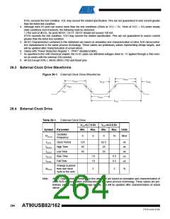
26.3 External Clock Drive Waveforms
Figure 26-1. External Clock Drive Waveforms
VIH1
VIL1
26.4 External Clock Drive
Table 26-1. External Clock Drive
VCC=2.7-5.5V
VCC=4.5-5.5V
Symbol Parameter
Min.
Max.
Min.
Max.
Units
Oscillator
1/tCLCL
0
8
0
16
MHz
Frequency
tCLCL
tCHCX
tCLCX
tCLCH
tCHCL
Clock Period
High Time
Low Time
Rise Time
Fall Time
125
50
62.5
25
ns
ns
ns
μs
μs
50
25
1.6
1.6
0.5
0.5
Change in period
from one clock
cycle to the next
ΔtCLCL
2
2
%
Note:
All DC Characteristics contained in this datasheet are based on simulation and characterization of
other AVR microcontrollers manufactured in the same process technology. These values are pre-
liminary values representing design targets, and will be updated after characterization of actual
silicon.
264
AT90USB82/162
7707D–AVR–07/08

 ATMEL [ ATMEL ]