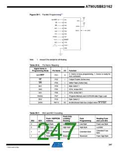
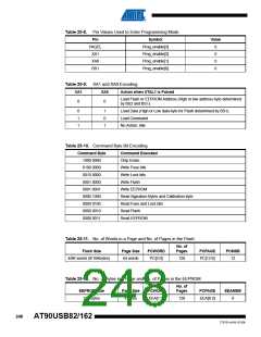
Table 25-8. Pin Values Used to Enter Programming Mode
Pin
PAGEL
XA1
Symbol
Value
Prog_enable[3]
Prog_enable[2]
Prog_enable[1]
Prog_enable[0]
0
0
0
0
XA0
BS1
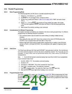
Table 25-9. XA1 and XA0 Encoding
XA1
XA0
Action when XTAL1 is Pulsed
Load Flash or EEPROM Address (High or low address byte determined
by BS2 and BS1).
0
0
0
1
1
1
0
1
Load Data (High or Low data byte for Flash determined by BS1).
Load Command
No Action, Idle
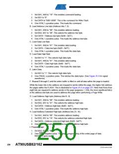
Table 25-10. Command Byte Bit Encoding
Command Byte
1000 0000
0100 0000
0010 0000
0001 0000
0001 0001
0000 1000
0000 0100
0000 0010
0000 0011
Command Executed
Chip Erase
Write Fuse bits
Write Lock bits
Write Flash
Write EEPROM
Read Signature Bytes and Calibration byte
Read Fuse and Lock bits
Read Flash
Read EEPROM
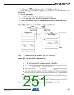
Table 25-11. No. of Words in a Page and No. of Pages in the Flash
No. of
Flash Size
Page Size
PCWORD
Pages
PCPAGE
PCMSB
4/8K words (8/16Kbytes)
64 words
PC[5:0]
128
PC[12:6]
12
Table 25-12. No. of Bytes in a Page and No. of Pages in the EEPROM
No. of
EEPROM Size
Page Size
PCWORD
Pages
PCPAGE
EEAMSB
512 bytes
4 bytes
EEA[1:0]
128
EEA[8:2]
8
248
AT90USB82/162
7707D–AVR–07/08

 ATMEL [ ATMEL ]