AT90USB82/162
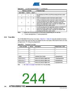
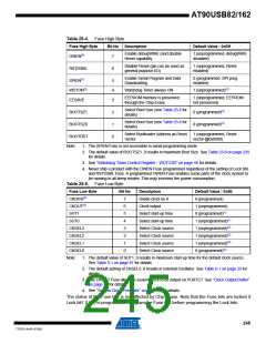
Table 25-4. Fuse High Byte
Fuse High Byte
Bit No
Description
Default Value : 0xD9
Enable debugWIRE (and disable
Reset capability
1 (unprogrammed, debugWIRE
disabled)
DWEN(4)
7
Disable Reset (pin can be used as
general purpose I/O)
1 (unprogrammed, Reset
enabled)
RSTDSBL
6
Enable Serial Program and Data
Downloading
0 (programmed, SPI prog.
enabled)
SPIEN(1)
WDTON(3)
EESAVE
5
4
3
Watchdog Timer always ON
1 (unprogrammed)(3)
EEPROM memory is preserved
through the Chip Erase
1 (unprogrammed, EEPROM
not preserved)
Select Boot Size (see Table 25-6 for
details)
BOOTSZ1
BOOTSZ0
BOOTRST
2
1
0
0 (programmed)(2)
0 (programmed)(2)
Select Boot Size (see Table 25-6 for
details)
Select Bootloader Address as Reset
Vector
1 (unprogrammed, Reset
vector @0x0000)
Note:
1. The SPIEN Fuse is not accessible in serial programming mode.
2. The default value of BOOTSZ1..0 results in maximum Boot Size. See Table 23-8 on page 239
for details.
3. See “Watchdog Timer Control Register - WDTCSR” on page 56 for details.
4. Never ship a product with the DWEN Fuse programmed regardless of the setting of Lock bits
and RSTDSBL Fuse. A programmed DWEN Fuse enables some parts of the clock system to
be running in all sleep modes. This may increase the power consumption.
Table 25-5. Fuse Low Byte
Fuse Low Byte
CKDIV8(4)
CKOUT(3)
SUT1
Bit No
Description
Default Value : 0x5E
0 (programmed)
7
6
5
4
3
2
1
0
Divide clock by 8
Clock output
1 (unprogrammed)
0 (programmed)(1)
1 (unprogrammed)(1)
1 (unprogrammed)(2)
1 (unprogrammed)(2)
1 (unprogrammed)(2)
0 (programmed)(2)
Select start-up time
Select start-up time
Select Clock source
Select Clock source
Select Clock source
Select Clock source
SUT0
CKSEL3
CKSEL2
CKSEL1
CKSEL0
Note:
1. The default value of SUT1..0 results in maximum start-up time for the default clock source.
See Table 9-1 on page 47 for details.
2. The default setting of CKSEL3..0 results in external Oscillator. See Table 6-1 on page 29 for
details.
3. The CKOUT Fuse allow the system clock to be output on PORTC7. See “Clock Output Buffer”
on page 34 for details.
4. See “System Clock Prescaler” on page 34 for details.
The status of the Fuse bits is not affected by Chip Erase. Note that the Fuse bits are locked if
Lock bit1 (LB1) is programmed. Program the Fuse bits before programming the Lock bits.
245
7707D–AVR–07/08

 ATMEL [ ATMEL ]