AT90USB82/162
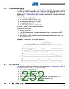
3. Wait until RDY/BSY goes high (See Figure 25-3 for signal waveforms).
J. Repeat B through I until the entire Flash is programmed or until all data has been
programmed.
K. End Page Programming
1. 1. Set XA1, XA0 to “10”. This enables command loading.
2. Set DATA to “0000 0000”. This is the command for No Operation.
3. Give XTAL1 a positive pulse. This loads the command, and the internal write signals
are reset.
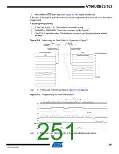
Figure 25-2. Addressing the Flash Which is Organized in Pages(1)
PCMSB
PAGEMSB
PCWORD
PROGRAM
COUNTER
PCPAGE
PAGE ADDRESS
WITHIN THE FLASH
WORD ADDRESS
WITHIN A PAGE
PROGRAM MEMORY
PAGE
PAGE
INSTRUCTION WORD
PCWORD[PAGEMSB:0]:
00
01
02
PAGEEND
Note:
1. PCPAGE and PCWORD are listed in Table 25-11 on page 248.
Figure 25-3. Programming the Flash Waveforms(1)
F
A
B
C
D
E
B
C
D
E
G
I
H
0x10
ADDR. LOW
DATA LOW
DATA HIGH
ADDR. LOW DATA LOW
DATA HIGH
ADDR. HIGH
ADDR. EXT.H
XX
XX
XX
DATA
XA1
XA0
BS1
BS2
XTAL1
WR
RDY/BSY
RESET +12V
OE
PAGEL
Note:
1. “XX” is don’t care. The letters refer to the programming description above.
251
7707D–AVR–07/08

 ATMEL [ ATMEL ]