AT90USB82/162
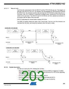
The RWAL bit always reflects the state of the current bank. This bit is set if the firmware can
write data to the bank, and cleared by hardware when the bank is full.
Example with 1 IN data bank
NAK
DATA
(bank 0)
IN
ACK
HW
IN
TXINI
SW
SW
write data from CPU
BANK 0
FIFOCON
SW
SW
write data from CPU
BANK 0
Example with 2 IN data banks
DATA
(bank 0)
DATA
(bank 1)
IN
ACK
HW
IN
ACK
TXINI
SW
SW
SW
write data from CPU
BANK0
write data from CPU
BANK 0
write data from CPU
BANK 1
FIFOCON
SW
SW
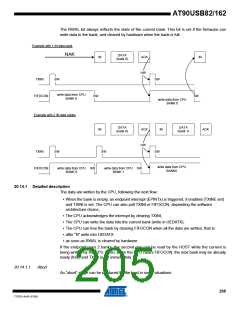
20.14.1 Detailed description
The data are written by the CPU, following the next flow:
• When the bank is empty, an endpoint interrupt (EPINTx) is triggered, if enabled (TXINE set)
and TXINI is set. The CPU can also poll TXINI or FIFOCON, depending the software
architecture choice,
• The CPU acknowledges the interrupt by clearing TXINI,
• The CPU can write the data into the current bank (write in UEDATX),
• The CPU can free the bank by clearing FIFOCON when all the data are written, that is:
• after “N” write into UEDATX
• as soon as RWAL is cleared by hardware.
If the endpoint uses 2 banks, the second one can be read by the HOST while the current is
being written by the CPU. Then, when the CPU clears FIFOCON, the next bank may be already
ready (free) and TXINI is set immediately.
20.14.1.1
Abort
An “abort” stage can be produced by the host in some situations:
205
7707D–AVR–07/08

 ATMEL [ ATMEL ]