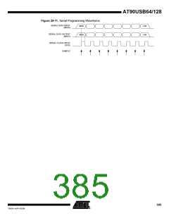
1. Power-up sequence:
Apply power between VCC and GND while RESET and SCK are set to “0”. In some sys-
tems, the programmer can not guarantee that SCK is held low during power-up. In this
case, RESET must be given a positive pulse of at least two CPU clock cycles duration
after SCK has been set to “0”.
2. Wait for at least 20 ms and enable serial programming by sending the Programming
Enable serial instruction to pin PDI.
3. The serial programming instructions will not work if the communication is out of syn-
chronization. When in sync. the second byte (0x53), will echo back when issuing the
third byte of the Programming Enable instruction. Whether the echo is correct or not, all
four bytes of the instruction must be transmitted. If the 0x53 did not echo back, give
RESET a positive pulse and issue a new Programming Enable command.
4. The Flash is programmed one page at a time. The memory page is loaded one byte at
a time by supplying the 7 LSB of the address and data together with the Load Program
Memory Page instruction. To ensure correct loading of the page, the data low byte must
be loaded before data high byte is applied for a given address. The Program Memory
Page is stored by loading the Write Program Memory Page instruction with the address
lines 15..8. Before issuing this command, make sure the instruction Load Extended
Address Byte has been used to define the MSB of the address. The extended address
byte is stored until the command is re-issued, i.e., the command needs only be issued
for the first page, and when crossing the 64KWord boundary. If polling (RDY/BSY) is not
used, the user must wait at least tWD_FLASH before issuing the next page. (See Table 29-
15.) Accessing the serial programming interface before the Flash write operation com-
pletes can result in incorrect programming.
5. The EEPROM array is programmed one byte at a time by supplying the address and
data together with the appropriate Write instruction. An EEPROM memory location is
first automatically erased before new data is written. If polling is not used, the user must
wait at least tWD_EEPROM before issuing the next byte. (See Table 29-15.) In a chip
erased device, no 0xFFs in the data file(s) need to be programmed.
6. Any memory location can be verified by using the Read instruction which returns the
content at the selected address at serial output PDO. When reading the Flash memory,
use the instruction Load Extended Address Byte to define the upper address byte,
which is not included in the Read Program Memory instruction. The extended address
byte is stored until the command is re-issued, i.e., the command needs only be issued
for the first page, and when crossing the 64KWord boundary.
7. At the end of the programming session, RESET can be set high to commence normal
operation.
8. Power-off sequence (if needed):
Set RESET to “1”.
Turn VCC power off.
Table 29-15. Minimum Wait Delay Before Writing the Next Flash or EEPROM Location
Symbol
Minimum Wait Delay
4.5 ms
tWD_FLASH
tWD_EEPROM
tWD_ERASE
9.0 ms
9.0 ms
384
AT90USB64/128
7593A–AVR–02/06

 ATMEL [ ATMEL ]