AT90USB64/128
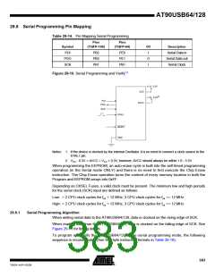
29.8 Serial Programming Pin Mapping
Table 29-14. Pin Mapping Serial Programming
Pins
Pins
Symbol
PDI
(TQFP-100)
(TQFP-64)
I/O
Description
Serial Data in
Serial Data out
Serial Clock
PB2
PE0
PE1
PB1
I
O
I
PDO
SCK
PB3
PB1
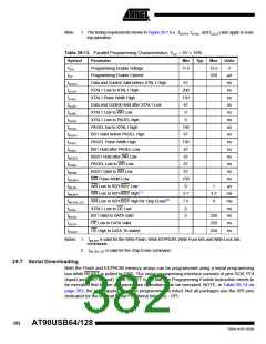
Figure 29-10. Serial Programming and Verify(1)
+1.8 - 5.5V
VCC
+1.8 - 5.5V(2)
PDI
AVCC
PDO
SCK
XTAL1
RESET
GND
Notes: 1. If the device is clocked by the internal Oscillator, it is no need to connect a clock source to the
XTAL1 pin.
2. VCC - 0.3V < AVCC < VCC + 0.3V, however, AVCC should always be within 1.8 - 5.5V
When programming the EEPROM, an auto-erase cycle is built into the self-timed programming
operation (in the Serial mode ONLY) and there is no need to first execute the Chip Erase
instruction. The Chip Erase operation turns the content of every memory location in both the
Program and EEPROM arrays into 0xFF.
Depending on CKSEL Fuses, a valid clock must be present. The minimum low and high periods
for the serial clock (SCK) input are defined as follows:
Low: > 2 CPU clock cycles for fck < 12 MHz, 3 CPU clock cycles for fck >= 12 MHz
High: > 2 CPU clock cycles for fck < 12 MHz, 3 CPU clock cycles for fck >= 12 MHz
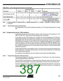
29.8.1
Serial Programming Algorithm
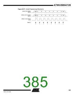
When writing serial data to the AT90USB64/128, data is clocked on the rising edge of SCK.
When reading data from the AT90USB64/128, data is clocked on the falling edge of SCK. See
Figure 29-11 for timing details.
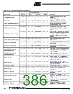
To program and verify the AT90USB64/128 in the serial programming mode, the following
sequence is recommended (See four byte instruction formats in Table 29-16):
383
7593A–AVR–02/06

 ATMEL [ ATMEL ]