AT89C5132
23.3.9.2
Timings
Table 124. External Clock AC Timings
VDD = 2.7 to 3.3V, TA= -40 to +85°C
Symbol
TCLCL
Parameter
Min
50
10
10
3
Max
Unit
ns
ns
ns
ns
ns
%
Clock Period
High Time
TCHCX
TCLCX
TCLCH
TCHCL
TCR
Low Time
Rise Time
Fall Time
3
Cyclic Ratio in X2 Mode
40
60
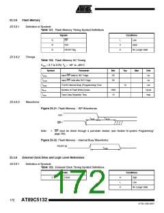
23.3.9.3
Waveforms
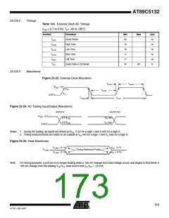
Figure 23-23. External Clock Waveform
TCLCH
TCHCX
VDD - 0.5
VIH1
TCLCX
VIL
0.45 V
TCHCL
TCLCL
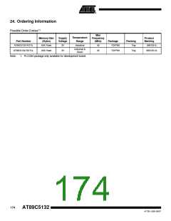
Figure 23-24. AC Testing Input/Output Waveforms
INPUTS
OUTPUTS
VIH min
VDD - 0.5
0.7 VDD
0.3 VDD
0.45 V
VIL max
Notes: 1. During AC testing, all inputs are driven at
V
DD -0.5V for a logic 1 and 0.45V for a logic 0.
2. Timing measurements are made on all outputs at VIH min for a logic 1 and VIL max for a logic 0.
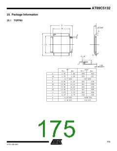
Figure 23-25. Float Waveforms
VLOAD + 0.1V
VLOAD - 0.1V
VOH - 0.1V
VOL + 0.1V
VLOAD
Timing Reference Points
Note:
For timing purposes, a port pin is no longer floating when a 100 mV change from load voltage occurs and begins to float when a
100 mV change from the loading VOH/VOL level occurs with IOL/IOH = 20 mA.
173
4173E–USB–09/07

 ATMEL [ ATMEL ]