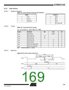
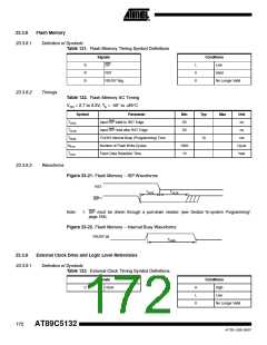
23.3.8
Flash Memory
23.3.8.1
Definition of Symbols
Table 121. Flash Memory Timing Symbol Definitions
Signals
ISP
Conditions
Low
S
R
B
L
V
X
RST
Valid
FBUSY flag
No Longer Valid
23.3.8.2
Timings
Table 122. Flash Memory AC Timing
DD = 2.7 to 3.3V, TA = -40° to +85°C
V
Symbol
TSVRL
Parameter
Min
50
Typ
Max
Unit
ns
Input ISP Valid to RST Edge
TRLSX
TBHBL
NFCY
TFDR
Input ISP Hold after RST Edge
FLASH Internal Busy (Programming) Time
Number of Flash Write Cycles
Flash Data Retention Time
50
ns
10
ms
100K
10
Cycle
Year
23.3.8.3
Waveforms
Figure 23-21. Flash Memory – ISP Waveforms
RST
TSVRL
TRLSX
ISP(1)
Note:
1. ISP must be driven through a pull-down resistor (see Section “In-system Programming”,
page 158).
Figure 23-22. Flash Memory – Internal Busy Waveforms
FBUSY bit
TBHBL
23.3.9
External Clock Drive and Logic Level References
23.3.9.1
Definition of Symbols
Table 123. External Clock Timing Symbol Definitions
Signals
Clock
Conditions
High
C
H
L
Low
X
No Longer Valid
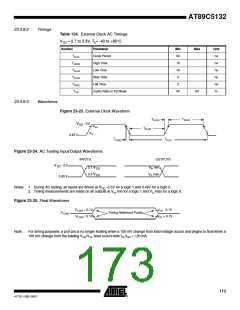
172
AT89C5132
4173E–USB–09/07

 ATMEL [ ATMEL ]