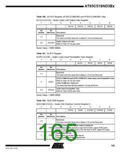
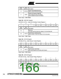
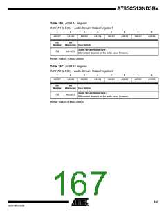
AT85C51SND3Bx
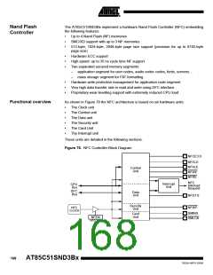
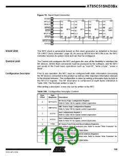
Figure 79. Nand Flash Connection
IOVDD
VDD
VDD
VDD
VDD
CLE
CLE
ALE
CLE
ALE
CLE
ALE
NFCLE
ALE
NFALE
WE
WE
RE
WE
RE
WE
RE
NFWE
NF3
SMC
NF0
NF1
NF2
RE
NFRE
D7:0
D7:0
D7:0
D7:0
NFD7:0
WP
NFWP
WP
WP
WP
CE VSS
CE VSS
1
CE VSS
2
CE VSS
3
0
NFCE3:0
IOVSS
Clock Unit
The NFC clock is generated based on the clock generator as detailed in Section
"DFC/NFC Clock Generator", page 30. As soon as NFEN bit in NFCON is set, the NFC
controller receives its system clock and can then be configured.
Control Unit
The Control unit configures the NFC and gives the user all the flexibility to interface the
NF devices. All the flash commands must be produced by the software, and the NFC
just sends to the Flash basic operations such as “read Id”, “write a byte”, “erase a
block”, …
Configuration Descriptor
Prior to any operation, the NFC must be configured with static information concerning
the NF devices connected to the product as well as other important information relevant
to the desired behavior. The configuration is done by writing a descriptor byte by byte in
the NFCFG register. The NF descriptor is composed of eight bytes (detailed in
Table 188). The first byte written is byte 0.
After writing a descriptor, a new one can be written to the NFC.
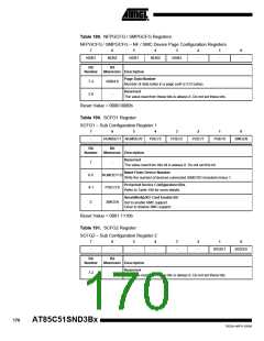
Table 188. Configuration Descriptor Content
Byte
Byte
Offset
Mnemonic Description
NF Device Page Configuration Register
0
1
2
NFPGCFG
SMPGCFG
SCFG1
Refer to Table 189 for register content organization.
SMC Device Page Configuration Register
Refer to Table 189 for register content organization.
Sub Configuration Register 1
Refer to Table 190 for register content organization.
Sub Configuration Register 2
3
4
SCFG2
FPBH
Refer to Table 191 for register content organization.
NF Device First Protected Block Address Registers
First address block of protected area. Refer to Section “Write Protection” for
detailed information.
Reset Value is 0000 0000b, 0000 0000b.
5
6
7
FPBL
LPBH
LPBL
NF Device Last Protected Block Address Registers
First address block of protected area. Refer to Section “Write Protection” for
detailed information.
Reset Value is 0000 0000b, 0000 0000b.
169
7632A–MP3–03/06

 ATMEL [ ATMEL ]