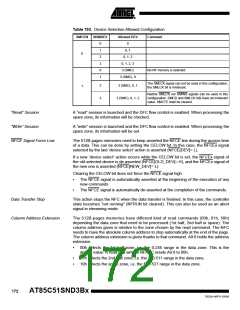
Nand Flash
Controller
The AT85C51SND3Bx implement a hardware Nand Flash Controller (NFC) embedding
the following features:
•
•
•
Up to 4 Nand Flash (NF) memories
SMC/XD support with up to 3 NF memories
512-byte, 1024-byte, 2048-byte page size support (provision for up to 8192-byte
page size)
•
•
•
Hardware ECC support
High speed: up to 35 ns cycle time NF support
Two separated secured memory segments:
–
–
application segment for user codes, audio codec codes, fonts, screens…
mass storage segment for FAT formatting
•
•
•
Hardware write protection management for application code segment
Very high data transfer rate in read and write using DFC interface
Proprietary wear-levelling support with extremely reduced CPU load
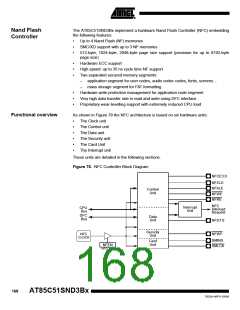
Functional overview
As shown in Figure 78 the NFC architecture is based on six hardware units:
•
•
•
•
•
•
The Clock unit
The Control unit
The Data unit
The Security unit
The Card Unit
The Interrupt unit
These units are detailed in the following sections.
Figure 78. NFC Controller Block Diagram
NFCE3:0
NFCLE
NFALE
NFWE
NFRE
Control
Unit
NFC
Interrupt
Unit
CPU
Bus
DFC
Bus
Interrupt
Request
Data
Unit
NFD7:0
Security
Unit
NFC
CLOCK
NFWP
SMINS
SMLCK
Card
Unit
NFEN
NFCON.0
168
AT85C51SND3Bx
7632A–MP3–03/06

 ATMEL [ ATMEL ]