AT8xC51SND2C
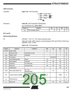
USB Connection
Schematic
Figure 144. USB Connection
To Power Supply
RUSB
VBUS
D+
D-
D+
D-
RUSB
GND
VSS
Parameters
Table 185. USB Termination Characteristics
DD = 2.7 to 3.3 V, TA = -40 to +85°C
V
Symbol
Parameter
USB Termination Resistor
Min
Typ
Max
Unit
RUSB
27
Ω
DAC and PA
Electrical Specifications
PA
AUDVBAT = 3.6V, TA = 25°C unless otherwise noted.
High power mode, 100nF capacitor connected between CBP and AUDVSS, 470nF input
capacitors, Load = 8 ohms.
Figure 145. PA Specification
Symbol
Parameter
Conditions
Min
3.2
-
Typ
Max
5.5
8
Unit
V
AUDVBAT Supply Voltage
-
IDD
IDDstby
VCBP
VOS
ZIN
Quiescent Current
Standby Current
DC Reference
Inputs shorted, no load
6
mA
µA
V
Capacitance
-
-
2
-
AUDVBAT/2
-
Output differential offset
Input impedance
Output load
full gain
-20
12K
6
0
20k
8
20
30k
32
300
100
mV
W
Active state
ZLFP
ZLLP
CL
Full Power mode
Low-Power mode
W
Output load
100
-
150
-
W
Capacitive load
pF
200 – 2kHz
PSRR
BW
Power supply rejection ratio
Output Frequency bandwidth
-
60
-
-
dB
Hz
Differential output
1KHz reference frequency
3dB attenuation.
50
20000
470nF input coupling capacitors
Off to on mode. Voltage already settled.
Input capacitors precharged
tUP
VN
Output setup time
Output noise
-
-
-
10
ms
Max gain, A weighted
120
500
µVRMS
205
4341D–MP3–04/05

 ATMEL [ ATMEL ]