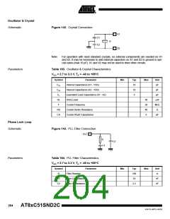
Oscillator & Crystal
Schematic
Figure 142. Crystal Connection
X1
X2
C1
C2
Q
VSS
Note:
For operation with most standard crystals, no external components are needed on X1
and X2. It may be necessary to add external capacitors on X1 and X2 to ground in spe-
cial cases (max 10 pF). X1 and X2 may not be used to drive other circuits.
Parameters
Table 183. Oscillator & Crystal Characteristics
DD = 2.7 to 3.3 V, TA = -40 to +85°C
V
Symbol
CX1
CX2
CL
Parameter
Internal Capacitance (X1 - VSS)
Internal Capacitance (X2 - VSS)
Equivalent Load Capacitance (X1 - X2)
Drive Level
Min
Typ
10
10
5
Max
Unit
pF
pF
pF
DL
50
20
40
6
µW
MHz
Ω
F
Crystal Frequency
RS
Crystal Series Resistance
Crystal Shunt Capacitance
CS
pF
Phase Lock Loop
Schematic
Figure 143. PLL Filter Connection
FILT
R
C2
C1
VSS
VSS
Parameters
Table 184. PLL Filter Characteristics
DD = 2.7 to 3.3 V, TA = -40 to +85°C
V
Symbol
R
Parameter
Min
Typ
100
10
Max
Unit
Ω
Filter Resistor
C1
Filter Capacitance 1
Filter Capacitance 2
nF
nF
C2
2.2
204
AT8xC51SND2C
4341D–MP3–04/05

 ATMEL [ ATMEL ]