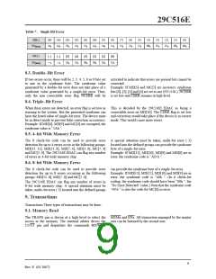
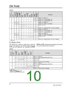
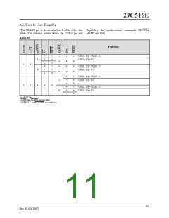
29C516E
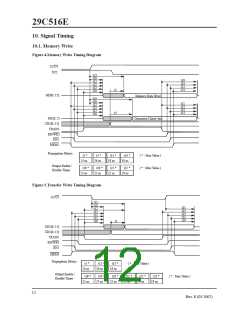
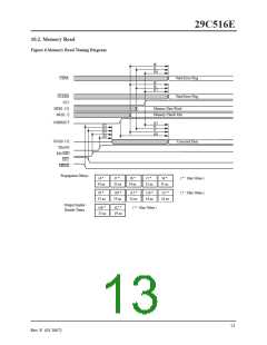
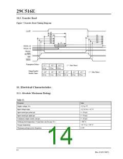
10.3. Transfer Read
Figure 7.Transfer Read Timing Diagram
U2/U1
t13
t20
t12
t22
t22
t22
t18
t21
t23
t23
t23
t19
t1
UD2[0..15]
UD1[0..15]
TRANS
RD/WR2
EN2
MEM2
Propagation Delays
t1 *
t12 *
20 ns
t13 *
( * : Max Value )
14 ns
18 ns
Output Enable /
Disable Times
t18 *
23 ns
t19 *
23 ns
t20 *
22 ns
t21 *
22 ns
t22 *
19 ns
t23 *
19 ns
( * : Max Value )
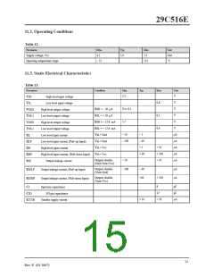
11. Electrical Characteristics
11.1. Absolute Maximum Ratings
Table 11:
Parameter
Value
Supply voltage, Vcc
– 0.5 to 7V
Input voltage range
– 0.5 to Vcc + 0.5 V
+/– 50 mA
Input current per power pin
Input current per signal pin
+/– 10 mA
Continuous output current, one pin
Soldering lead temperature 1.6 mm from case for max 10 s
Storage temperature
+/– 30 mA
ꢀ
+ 300
C
ꢀ
ꢀ
– 65 C to + 150
1.0 W
C
Maximum package power dissipation
14
Rev. E (03 2007)

 ATMEL [ ATMEL ]