AT29C020
AC Read Characteristics
AT29C020-90 AT29C020-10 AT29C020-12 AT29C020-15
Min
Max
90
90
40
25
Min
Max
100
100
50
Min
Max
120
120
50
Min
Max
150
150
70
Symbol Parameter
Units
ns
t
t
t
t
Address to Output Delay
CE to Output Delay
0
ACC
(1)
ns
CE
OE
DF
(2)
OE to Output Delay
0
0
0
0
0
0
0
0
ns
(3, 4)
CE or OE to Output Float
25
30
40
ns
Output Hold from OE, CE or
Address, whichever
occurred first
t
0
0
0
0
ns
OH
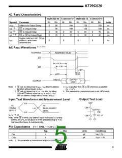
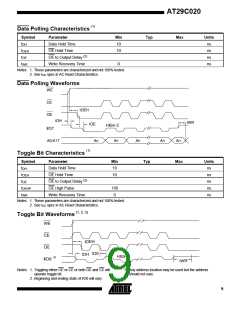
AC Read Waveforms (1, 2, 3, 4)
Notes: 1. CE may be delayed up to tACC - tCE after the address
transition without impact on tACC
3. tDF is specified from OE or CE whichever occurs first
(CL = 5 pF).
.
2. OE may be delayed up to tCE - tOE after the falling
edge of CE without impact on tCE or by tACC - tOE
4. This parameter is characterized and is not 100% tested.
after an address change without impact on tACC
.
Output Test Load
Input Test Waveforms and Measurement Level
t , t < 5 ns
R
F
Note: While CE is active, any address inputs that cause VIH to drop
below 2.0V or VIL to rise above 0.8V for a duration of up to 15 ns
may cause the device to read incorrectly.
Pin Capacitance (f = 1 MHz, T = 25°C) (1)
Typ
Max
6
Units
pF
Conditions
C
C
4
8
V
V
= 0V
IN
IN
12
pF
= 0V
OUT
OUT
Note: 1. This parameter is characterized and is not 100% tested.
5

 ATMEL [ ATMEL ]