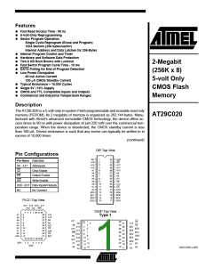
Description (Continued)
To allow for simple in-system reprogrammability, the
AT29C020 does not require high input voltages for pro-
gramming. Five-volt-only commands determine the opera-
tion of the device. Reading data out of the device is similar
to reading from an EPROM. Reprogramming the
AT29C020 is performed on a sector basis; 256-bytes of
data are loaded into the device and then simultaneously
programmed.
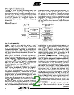
During a reprogram cycle, the address locations and 256-
bytes of data are internally latched, freeing the address
and data bus for other operations. Following the initiation
of a program cycle, the device will automatically erase the
sector and then program the latched data using an internal
control timer. The end of a program cycle can be detected
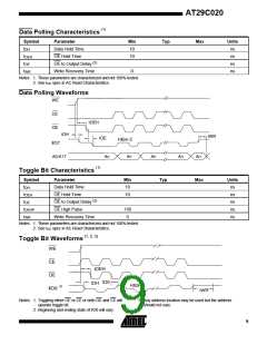
by DATA polling of I/O7. Once the end of a program cycle
has been detected, a new access for a read or program
can begin.
Block Diagram
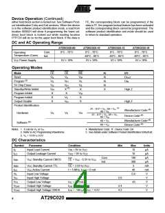
Device Operation
period will start. A8 to A17 specify the sector address. The
sector address must be valid during each high to low tran-
sition of WE (or CE). A0 to A7 specify the byte address
within the sector. The bytes may be loaded in any order;
sequential loading is not required. Once a programming
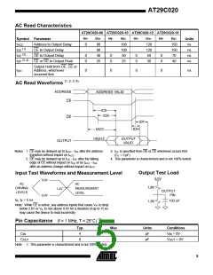
READ: The AT29C020 is accessed like an EPROM.
When CE and OE are low and WE is high, the data stored
at the memory location determined by the address pins is
asserted on the outputs. The outputs are put in the high
impedance state whenever CE or OE is high. This dual-
line control gives designers flexibility in preventing bus
contention.
operation has been initiated, and for the duration of t , a
WC
read operation will effectively be a polling operation.
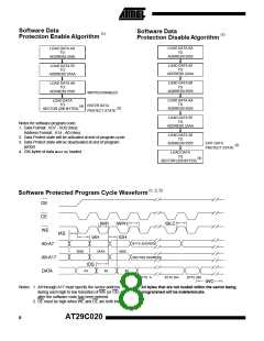
SOFTWARE DATA PROTECTION: A software control-
led data protection feature is available on the AT29C020.
Once the software protection is enabled a software algo-
rithm must be issued to the device before a program may
be performed. The software protection feature may be en-
abled or disabled by the user; when shipped from Atmel,
the software data protection feature is disabled. To enable
the software data protection, a series of three program
commands to specific addresses with specific data must
be performed. After the software data protection is en-
abled the same three program commands must begin
each program cycle in order for the programs to occur. All
software program commands must obey the sector pro-
gram timing specifications. Once set, the software data
protection feature remains active unless its disable com-
mand is issued. Power transitions will not reset the soft-
ware data protection feature, however the software fea-
ture will guard against inadvertent program cycles during
power transitions.
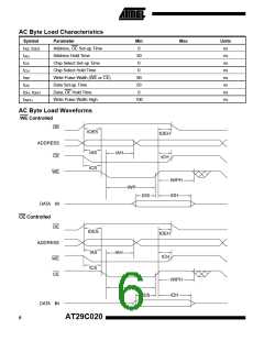
BYTE LOAD: Byte loads are used to enter the 256-
bytes of a sector to be programmed or the software codes
for data protection. A byte load is performed by applying a
low pulse on the WE or CE input with CE or WE low (re-
spectively) and OE high. The address is latched on the
falling edge of CE or WE, whichever occurs last. The data
is latched by the first rising edge of CE or WE.
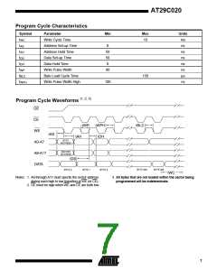
PROGRAM: The device is reprogrammed on a sector
basis. If a byte of data within a sector is to be changed,
data for the entire sector must be loaded into the device.
Any byte that is not loaded during the programming of its
sector will be indeterminate. Once the bytes of a sector
are loaded into the device, they are simultaneously pro-
grammed during the internal programming period. After
the first data byte has been loaded into the device, suc-
cessive bytes are entered in the same manner. Each new
byte to be programmed must have its high to low transition
on WE (or CE) within 150 µs of the low to high transition of
WE (or CE) of the preceding byte. If a high to low transition
is not detected within 150 µs of the last low to high transi-
tion, the load period will end and the internal programming
After setting SDP, any attempt to write to the device with-
out the 3-byte command sequence will start the internal
(continued)
2
AT29C020

 ATMEL [ ATMEL ]