AT29C020
Device Operation (Continued)
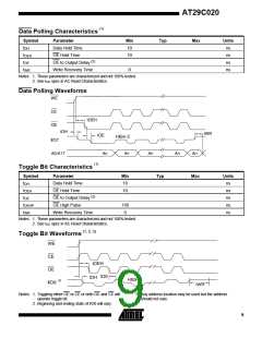
write timers. No data will be written to the device; however,
the program cycle has been completed, true data is valid
on all outputs and the next cycle may begin. DATA polling
may begin at any time during the program cycle.
for the duration of t , a read operation will effectively be
WC
a polling operation.
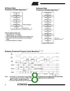
After the software data protection’s 3-byte command code
is given, a sector of data is loaded into the device using the
sector program timing specifications.
TOGGLE BIT: In addition to DATA polling the
AT29C020 provides another method for determining the
end of a program or erase cycle. During a program or
erase operation, successive attempts to read data from
the device will result in I/O6 toggling between one and
zero. Once the program cycle has completed, I/O6 will
stop toggling and valid data will be read. Examining the
toggle bit may begin at any time during a program cycle.
HARDWARE DATA PROTECTION: Hardware features
protect against inadvertent programs to the AT29C020 in
the following ways: (a) V sense— if V is below 3.8V
CC
CC
(typical), the program function is inhibited. (b) V power
CC
on delay— once V
has reached the V
sense level,
CC
CC
the device will automatically time out 5 ms (typical) before
programming. (c) Program inhibit— holding any one of OE
low, CE high or WE high inhibits program cycles. (d) Noise
filter— pulses of less than 15 ns (typical) on the WE or CE
inputs will not initiate a program cycle.
OPTIONAL CHIP ERASE MODE: The entire device
can be erased by using a 6-byte software code. Please
see Software Chip Erase application note for details.
BOOT BLOCK PROGRAMMING LOCKOUT: The
AT29C020 has two designated memory blocks that have
a programming lockout feature. This feature prevents pro-
gramming of data in the designated block once the feature
has been enabled. Each of these blocks consists of 8K
bytes; the programming lockout feature can be set inde-
pendently for either block. While the lockout feature does
not have to be activated, it can be activated for either or
both blocks.
PRODUCT IDENTIFICATION: The product identifica-
tion mode identifies the device and manufacturer as At-
mel. It may be accessed by hardware or software opera-
tion. The hardware operation mode can be used by an ex-
ternal programmer to identify the correct programming al-
gorithm for the Atmel product. In addition, users may wish
to use the software product identification mode to identify
the part (i.e. using the device code), and have the system
software use the appropriate sector size for program op-
erations. In this manner, the user can have a common
board design for 256K to 4-megabit densities and, with
each density’s sector size in a memory map, have the sys-
tem software apply the appropriate sector size.
These two 8K memory sections are referred to as boot
blocks. Secure code which will bring up a system can be
contained in a boot block. The AT29C020 blocks are lo-
cated in the first 8K bytes of memory and the last 8K bytes
of memory. The boot block programming lockout feature
can therefore support systems that boot from the lower
addresses of memory or the higher addresses. Once the
programming lockout feature has been activated, the data
in that block can no longer be erased or programmed;
data in other memory locations can still be changed
through the regular programming methods. To activate the
lockout feature, a series of seven program commands to
specific addresses with specific data must be performed.
Please see Boot Block Lockout Feature Enable Algorithm.
For details, see Operating Modes (for hardware operation)
or Software Product Identification. The manufacturer and
device code is the same for both modes.
DATA POLLING: The AT29C020 features DATA poll-
ing to indicate the end of a program cycle. During a pro-
gram cycle an attempted read of the last byte loaded will
result in the complement of the loaded data on I/O7. Once
If the boot block lockout feature has been activated on
either block, the chip erase function will be disabled.
Absolute Maximum Ratings*
Temperature Under Bias................. -55°C to +125°C
Storage Temperature...................... -65°C to +150°C
BOOT BLOCK LOCKOUT DETECTION: A software
method is available to determine whether programming of
(continued)
All Input Voltages
(including NC Pins)
with Respect to Ground ................... -0.6V to +6.25V
*NOTICE: Stresses beyond those listed under “Absolute Maxi-
mum Ratings” may cause permanent damage to the device.
This is a stress rating only and functional operation of the
device at these or any other conditions beyond those indi-
cated in the operational sections of this specification is not
implied. Exposure to absolute maximum rating conditions
for extended periods may affect device reliability.
All Output Voltages
with Respect to Ground .............-0.6V to V
+ 0.6V
CC
Voltage on OE
with Respect to Ground ................... -0.6V to +13.5V
3

 ATMEL [ ATMEL ]