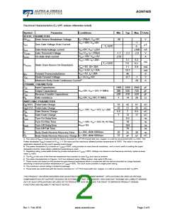
AON7405
Electrical Characteristics (TJ=25°C unless otherwise noted)
Symbol
Parameter
Conditions
Min
Typ
Max Units
STATIC PARAMETERS
ID=-250µA, VGS=0V
BVDSS
Drain-Source Breakdown Voltage
-30
V
VDS=-30V, VGS=0V
-1
µA
-5
IDSS
Zero Gate Voltage Drain Current
TJ=55°C
VDS=0V, VGS= ±25V
VDS=VGS ID=-250µA
VGS=-10V, VDS=-5V
VGS=-10V, ID=-20A
IGSS
Gate-Body leakage current
Gate Threshold Voltage
On state drain current
±100
-2.8
nA
V
VGS(th)
ID(ON)
-1.7
-2.2
-210
A
5.1
7.6
6.2
9.2
8.9
mΩ
TJ=125°C
RDS(ON)
Static Drain-Source On-Resistance
VGS=-6V, ID=-20A
7.1
mΩ
mΩ
S
VGS=-4.5V, ID=-10A
10.7
46
VDS=-5V, ID=-20A
IS=-1A,VGS=0V
Maximum Body-Diode Continuous CurrentG
gFS
VSD
IS
Forward Transconductance
Diode Forward Voltage
-0.7
-1
V
-50
A
DYNAMIC PARAMETERS
Ciss
Coss
Crss
Rg
Input Capacitance
1960 2450 2940
pF
pF
pF
Ω
VGS=0V, VDS=-15V, f=1MHz
Output Capacitance
Reverse Transfer Capacitance
Gate resistance
380
220
7
550
370
14
720
520
28
VGS=0V, VDS=0V, f=1MHz
SWITCHING PARAMETERS
Qg(10V) Total Gate Charge
33
16
5.5
7
42
21
7
51
26
8.5
17
nC
nC
nC
nC
ns
Qg(4.5V) Total Gate Charge
VGS=-10V, VDS=-15V, ID=-20A
Qgs
Qgd
tD(on)
tr
Gate Source Charge
Gate Drain Charge
Turn-On DelayTime
Turn-On Rise Time
Turn-Off DelayTime
Turn-Off Fall Time
12
9.5
10
104
78
VGS=-10V, VDS=-15V, RL=0.75Ω,
RGEN=3Ω
ns
tD(off)
tf
ns
ns
trr
IF=-20A, dI/dt=500A/µs
IF=-20A, dI/dt=500A/µs
20
37
Body Diode Reverse Recovery Time
Body Diode Reverse Recovery Charge
25
47
30
57
ns
Qrr
nC
A. The value of RθJA is measured with the device mounted on 1in2 FR-4 board with 2oz. Copper, in a still air environment with TA =25°C. The
Power dissipation PDSM is based on R θJA t ≤ 10s value and the maximum allowed junction temperature of 150°C. The value in any given
application depends on the user's specific board design.
B. The power dissipation PD is based on TJ(MAX)=150°C, using junction-to-case thermal resistance, and is more useful in setting the upper
dissipation limit for cases where additional heatsinking is used.
C. Repetitive rating, pulse width limited by junction temperature TJ(MAX)=150°C. Ratings are based on low frequency and duty cycles to keep
initial TJ =25°C.
D. The RθJA is the sum of the thermal impedence from junction to case RθJC and case to ambient.
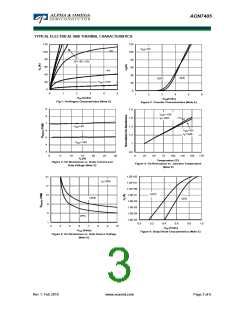
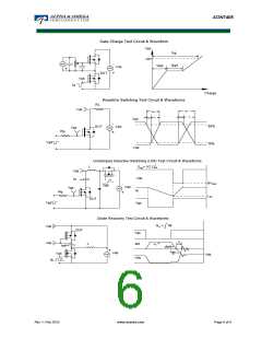
E. The static characteristics in Figures 1 to 6 are obtained using <300µs pulses, duty cycle 0.5% max.
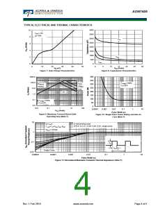
F. These curves are based on the junction-to-case thermal impedence which is measured with the device mounted to a large heatsink,
assuming a maximum junction temperature of TJ(MAX)=150°C. The SOA curve provides a single pulse ratin g.
G. The maximum current rating is limited by package.
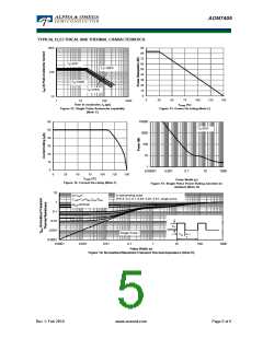
H. These tests are performed with the device mounted on 1 in2 FR-4 board with 2oz. Copper, in a still air environment with TA=25°C.
THIS PRODUCT HAS BEEN DESIGNED AND QUALIFIED FOR THE CONSUMER MARKET. APPLICATIONS OR USES AS CRITICAL
COMPONENTS IN LIFE SUPPORT DEVICES OR SYSTEMS ARE NOT AUTHORIZED. AOS DOES NOT ASSUME ANY LIABILITY ARISING
OUT OF SUCH APPLICATIONS OR USES OF ITS PRODUCTS. AOS RESERVES THE RIGHT TO IMPROVE PRODUCT DESIGN,
FUNCTIONS AND RELIABILITY WITHOUT NOTICE.
Rev 1: Feb 2010
www.aosmd.com
Page 2 of 6

 AOS [ ALPHA & OMEGA SEMICONDUCTORS ]