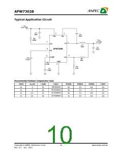
APW7302B
Application Information (Cont.)
Thermal Consideration
1. Begin the layout by placing the power components first.
Orient the power circuitry to achieve a clean power flow
path. If possible, make all the connections on one side of
the PCB with wide, copper filled areas.
The APW7302B maximum power dissipation depends
on the thermal resistance and temperature difference
between the die junction and ambient air. The power dis-
sipation PD across the device is:
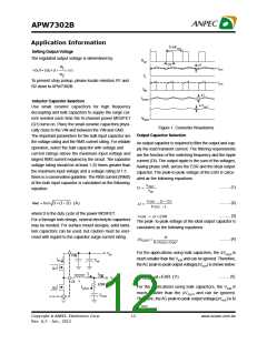
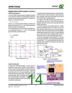
2. In Figure 3, the loops with same color bold lines con-
duct high slew rate current. These interconnecting im-
pedances should be minimized by using wide and short
printed circuit traces.
PD = (TJ - TA) / qJA
where (TJ-TA) is the temperature difference between the
junction and ambient air. qJA is the thermal resistance
between Junction and ambient air.
3. Keep the sensitive small signal nodes (FB, COMP)
away from switching nodes (LX or others) on the PCB
and it should be placed near the IC as close as possible.
Therefore, place the feedback divider and the feedback
compensation network close to the IC to avoid switching
noise. Connect the ground of feedback divider directly to
the GND pin of the IC using a dedicated ground trace.
4. Place the decoupling ceramic capacitor C1 near the
VIN as close as possible. Use a wide power ground plane
to connect the C1, C2, and Schottky diode to provide a low
impedance path between the components for large and
high slew rate current.
For normal operation, do not exceed the maximum junc-
tion temperature rating of TJ = 125oC. The calculated
power dissipation should less than:
PD = (125-25)/50
= 2(W)
2.5
2
+
SOP-8P
VIN
1.5
-
VIN
C1
BS
LX
L1
C3
EN
+
1
0.5
0
U1
Compensation
Network
Load VOUT
APW7302B
COMP
C2
-
R3
C5
FB
R1
GND
Feedback
Divider
R2
0
25
50
75
100
125
Ambient Temperature, TA(oC)
Figure 2. Current Path Diagram
Sensitive node (FB, COMP) should be away from
switching node(LX) and it should be placed near
the IC with short trace
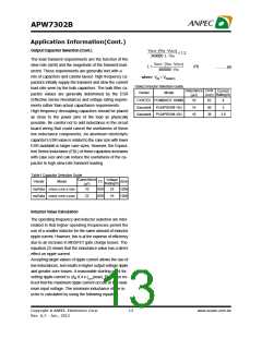
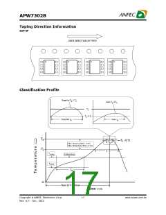
Layout Consideration
Numerous vias connected from
the thermal pad to the
solderside ground plane(s)
should be used to enhance heat
dissipation
Ground
In high power switching regulator, a correct layout is
important to ensure proper operation of the regulator. In
general, interconnecting impedance should be minimized
by using short, wide printed circuit traces. Signal and
power grounds are to be kept separating and finally
combined using the ground plane construction or single
point grounding. Figure 3 illustrates the layout, with bold
lines indicating high current paths. Components along
the bold lines should be placed close together. Below is
a checklist for your layout:
SOP-8
Input Capacitor C1 should be
near the IC as close as possible
VOUT
L1
VIN
VLX
C2
Power path should be short and wide
Figure 3. Recommended Layout Diagram
Copyright ã ANPEC Electronics Corp.
14
www.anpec.com.tw
Rev. A.2 - Jan., 2012

 ANPEC [ ANPEC ELECTRONICS COROPRATION ]