APW7302B
Application Information
T=1/FOSC
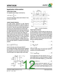
Setting Output Voltage
The regulated output voltage is determined by:
VLX
DT
I
R
1
IOUT
VOUT= 0.92´ (1+
) × (V)
R
IL
2
To prevent stray pickup, please locate resistors R1 and
R2 close to APW7302B.
IOUT
IQ1
I
ICOUT
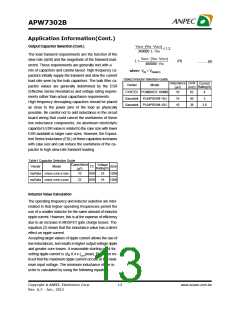
Inductor Capacitor Selection
VOUT
Use small ceramic capacitors for high frequency
decoupling and bulk capacitors to supply the surge cur-
rent needed each time the N-channel power MOSFET
(Q1) turns on. Place the small ceramic capacitors physi-
cally close to the VIN and between the VIN and GND.
The important parameters for the bulk input capacitor are
the voltage rating and the RMS current rating. For reliable
operation, select the bulk capacitor with voltage and
current ratings above the maximum input voltage and
largest RMS current required by the circuit. The capacitor
voltage rating should be at least 1.25 times greater than
the maximum input voltage and a voltage rating of 1.5
times is a conservative guideline. The RMS current (IRMS)
of the bulk input capacitor is calculated as the following
equation:
VOUT
Figure 1. Converter Waveforms
Output Capacitor Selection
An output capacitor is required to filter the output and sup-
ply the load transient current. The filtering requirements
are the function of the switching frequency and the ripple
current (DI). The output ripple is the sum of the voltages,
having phase shift, across the ESR and the ideal output
capacitor. The peak-to-peak voltage of the ESR is calcu-
ated as the following equations:
VOUT
........... (1)
D =
VIN
VOUT ´ (1 - D )
FOSC ´ L
........... (2)
........... (3)
IRMS = IOUT D ´ (1- D) ×(A)
DI =
where D is the duty cycle of the power MOSFET.
VESR = DI ´ ESR
For a through hole design, several electrolytic capacitors
may be needed. For surface mount designs, solid tanta-
lum capacitors can be used, but caution must be exer-
cised with regard to the capacitor surge current rating.
The peak- to-peak voltage of the ideal output capacitor is
calculated as the following equations:
DI
........... (4)
DVCOUT
=
8´ FOSC ´ COUT
For the applications using bulk capacitors, the DVCOUT is
much smaller than the VESR and can be ignored. Therefore,
theAC peak-to-peak output voltage(DVOUT) is shown below:
VIN
VIN
IQ1
CIN
Q1
Q2
IOUT
IL
........... (5)
DVOUT = DI´ ESR×(V)
VOUT
L
LX
ESR
COUT
For the applications using bulk capacitors, the VESR is
much smaller than the DVCOUT and can be ignored.
Therefore, the AC peak-to-peak output voltage(DVOUT) is to
ICOUT
DVCOUT
.
Copyright ã ANPEC Electronics Corp.
12
www.anpec.com.tw
Rev. A.2 - Jan., 2012

 ANPEC [ ANPEC ELECTRONICS COROPRATION ]