APA2069
Application Descriptions (Cont.)
does not eliminate the need for bypassing the supply
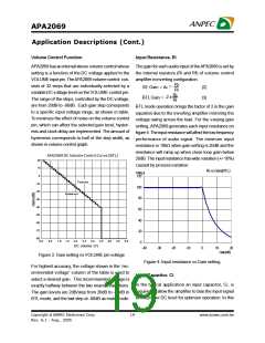
Input Capacitor, Ci (Cont.)
nodes of the APA2069. The selection of bypass
capacitors, especially Cbypass, is thus dependent
upon desired PSRR requirements, click and pop
performance.
case, Ci and the minimum input impedance Ri (10kW)
form a high-pass filter with the corner frequency
determined in the follow equation:
1
FC(highpass)=
(4)
To avoid start-up pop noise occurred, the bypass
voltage should rise slower than the input bias voltage
and the relationship shown in equation (6) should be
maintained.
2px10kWxCi
The value of Ci is important to consider as it directly
affects the low frequency performance of the circuit.
Consider the example where Ri is 10kW and the
specification calls for a flat bass response down to
1
1
<<
(6)
Cbypass x 125kW
100kW x Ci
100Hz. Equation is reconfigured as follow :
1
The bypass capacitor isfed thru from a 125kW resistor
inside the amplifier and the 100kW is maximum input
resistance of (Ri+ Rf). Bypass capacitor, Cb, values of
3.3mF to 10mF ceramic or tantalum low-ESR capacitors
are recommended for the best THD and noise
performance.
Ci=
(5)
2px10kWxfC
Consider to input resistance variation, the Ci is 0.16mF
so one would likely choose a value in the range
Afurther consideration for this capacitor is the leakage
path from the input source through the input network
(Ri+Rf, Ci) to the load. This leakage current creates a
DC offset voltage at the input to the amplifier that
reduces useful headroom, especially in high gain
applications. For this reason a low-leakage tantalum
or ceramiccapacitor isthe best choice. When polarized
capacitors are used, the positive side of the capacitor
should face the amplifier input in most applications as
theDC level thereisheld atVDD/2, whichislikelyhigher
that thesourceDC level. Pleasenotethat it isimportant
to confirm the capacitor polarity in the application.
The bypass capacitance also effects to the start up
time. It is determined in the following equation :
Tstart up = 5 x (Cbypass x 125KW)
(7)
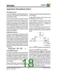
Output Coupling Capacitor, Cc
In the typical single-supply SE configuration, an
output coupling capacitor (Cc) is required to block the
DC bias at the output of the amplifier thus preventing
DC currents in the load. As with the input coupling
capacitor, the output coupling capacitor andimpedance
of theloadform ahigh-passfiltergovernedbyequation.
1
Effective BypassCapacitor, Cbypass
(8)
FC(highpass)=
2pRLCC
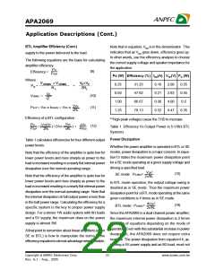
As other power amplifiers, proper supply bypassing is
critical for low noise performance and high power
supply rejection.
For example, a 330mF capacitor with an 8W speaker
would attenuate low frequencies below 60.6Hz. The
main disadvantage, from aperformance standpoint, is
the load impedance is typically small, which drives
the low-frequency corner higher degrading the bass
response. Large values of CC are required to passlow
frequencies into the load.
The capacitors located on both the bypass and power
supply pins should be as close to the device as
possible. The effect of a larger bypass capacitor will
improve PSRR due to increased supply stability.
Typical applicationsemploy a 5V regulator with 1.0mF
and a 0.1mF bypass capacitor as supply filtering. This
Copyright ã ANPEC Electronics Corp.
20
www.anpec.com.tw
Rev. A.1 - Aug., 2005

 ANPEC [ ANPEC ELECTRONICS COROPRATION ]