PRODUCT DATASHEET
AAT2601178
Total Power Solution for Portable Applications
Layout Guidance
Timer
Charger Watchdog Timer
0
1
ON (default)
OFF (and reset to zero)
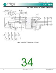
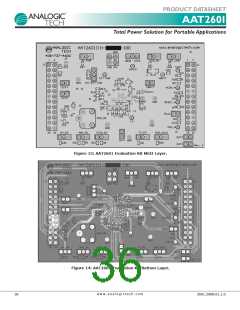
Figure 10 is the schematic for the evaluation board. The
evaluation board has extra components for easy evalua-
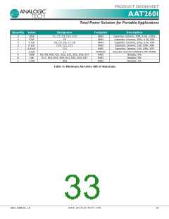
tion; the actual BOM need for a system is shown in Table
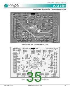
9. When laying out the PC board, the following layout
guideline should be followed to ensure proper operation
of the AAT2601:
Table 6: Timer Bit Setting for
the Charger Watchdog Timer.
LDO11
LDO10
LDO1 Output Voltage
1. The exposed pad EP must be reliably soldered to
PGND/AGND and multilayer GND. The exposed ther-
mal pad should be connected to board ground plane
and pins 2 and 16. The ground plane should include
a large exposed copper pad under the package with
VIAs to all board layers for thermal dissipation.
2. The power traces, including GND traces, the LX
traces and the VIN trace should be kept short, direct
and wide to allow large current flow. The L1 connec-
tion to the LX pins should be as short as possible.
Use several via pads when routing between layers.
3. The input capacitors (C1 and C2) should be con-
nected as close as possible to CHGIN (Pin 28) and
PGND (Pin 2) to get good power filtering.
0
0
1
1
0
1
0
1
3.00V (default)
2.90V
2.85V
2.80V
LDO21
LDO20
LDO2 Output Voltage
0
0
1
1
0
1
0
1
3.00V (default)
2.90V
2.85V
2.80V
LDO31
LDO30
LDO3 Output Voltage
0
0
1
1
0
1
0
1
3.00V (default)
2.90V
2.85V
2.80V
4. Keep the switching node LX away from the sensitive
OUTBUCK feedback node.
LDO41
LDO40
LDO4 Output Voltage
0
0
1
1
0
1
0
1
3.00V (default)
2.90V
5. The feedback trace for the OUTBUCK pin should be
separate from any power trace and connected as
closely as possible to the load point. Sensing along a
high current load trace will degrade DC load regula-
tion.
6. The output capacitor C4 and L1 should be connected
as close as possible and there should not be any
signal lines under the inductor.
2.85V
2.80V
LDO51
LDO50
LDO5 Output Voltage
0
0
1
1
0
1
0
1
3.00V (default)
2.90V
2.85V
2.80V
7. The resistance of the trace from the load return to
the PGND (Pin 2) should be kept to a minimum. This
will help to minimize any error in DC regulation due
to differences in the potential of the internal signal
ground and the power ground.
Table 7: LDO Bit Setting for
LDO Output Voltage Level.
SYS Bit
SYSOUT Power Source
If USE_USB = H, SYSOUT powered from BAT
If USE_USB = L, SYSOUT powered from CHGIN
0
1
SYSOUT always powered from BAT
Table 8: SYS Bit Setting for SYSOUT Power Path.
w w w . a n a l o g i c t e c h . c o m
32
2601.2008.01.1.0

 ANALOGICTECH [ ADVANCED ANALOGIC TECHNOLOGIES ]