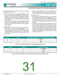
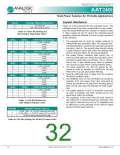
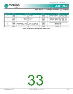
PRODUCT DATASHEET
AAT2601178
Total Power Solution for Portable Applications
I2C Serial Interface
and Programmability
The timing diagram in Figure 7 depicts the transmission
protocol.
START and STOP Conditions
Serial Interface
START and STOP conditions are always generated by the
master. Prior to initiating a START condition, both the
SDA and SCL pin are idle mode (idle mode is when there
is no activity on the bus and SDA and SCL are pulled to
VCC via external resistor). As depicted in Figure 7, a
START condition is defined to be when the master pulls
the SDA line low and after a short period pulls the SCL
line low. A START condition acts as a signal to all IC’s
that something is about to be transmitted on the BUS.
Many of the features of the AAT2601 can be controlled via
the I2C serial interface. The I2C serial interface is a wide-
ly used interface where it requires a master to initiate all
the communications with the slave devices. The I2C pro-
tocol consists of 2 active wire SDA (serial data line) and
SCL (serial clock line). Both wires are open drain and
require an external pull up resistor to VCC (SYSOUT may
be used as VCC). The SDA pin serves I/O function, and the
SCL pin controls and references the I2C bus. I2C protocol
is a bidirectional bus which allows both read and write
actions to take place, but the AAT2601 supports the write
protocol only. Since the protocol has a dedicated bit for
Read or Write access (R/W), when communicating with
AAT2601, this bit must be set to “0”.
A STOP condition, also shown in Figure 7, is when the
master releases the bus and SCL changes from low to
high followed by SDA low to high transition. The master
does not issue an ACKNOWLEGE and releases the SCL
and SDA pins.
ACK from slave
ACK from slave
ACK from slave
Chip
Address
Register
Address
START MSB
LSB
W
ACK MSB
LSB ACK MSB
Data
LSB ACK STOP
SCL
SDA
1
0
0
1
1
0
0
0
including R/W bit,
Chip Address = 0x98
Figure 7: I2C Timing Diagram.
w w w . a n a l o g i c t e c h . c o m
2601.2008.01.1.0
29

 ANALOGICTECH [ ADVANCED ANALOGIC TECHNOLOGIES ]