PRODUCT DATASHEET
AAT2601178
Total Power Solution for Portable Applications
address including the R/W bit is 0x98 (hex) or
10011000 in binary.
Transferring Data
Every byte on the bus must be 8 bits long. A byte is
always sent with a most significant bit first (see Figure
8).
Acknowledge Bit
The acknowledge bit is the ninth bit of data. It is used
to send back a confirmation to the master that the
data has been received properly. For acknowledge to
take place, the MASTER must first release the SDA
line, then the SLAVE will pull the data line low as
shown in Figure 7.
MSB
LSB
R/W
Figure 8: Bit Order.
The address is embedded in the first seven bits of the
byte. The eighth bit is reserved for the direction of the
information flow for the next byte of information. For
the AAT2601, this bit must be set to “0”. The full 8-bit
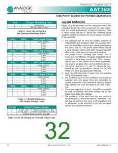
Serial Programming Code
After sending the chip address, the master should send
an 8-bit data stream to select which register to program
and then the codes that the user wishes to enter.
Register 0x00:
Timer
RCHG1
Not used
LDO50
RCHG0
Not used
LDO41
CHG2
Not used
LDO40
CHG1
Not used
LDO31
CHG0
SYS
Term1
LDO11
LDO21
Term0
LDO10
LDO20
Register 0x01:
Not used
Register 0x02:
LDO51
LDO30
Figure 9: Serial Programming Register Codes.
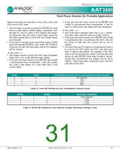
Constant Current Charge
Constant Current Charge as
% of ISET Current
USE_USB Pin
CHG2
CHG1
CHG0
ICH_CC
100mA
(fixed internally)
1
0
0
0
(default)
800mA
(set by ISET resistor)
0
0
0
0
100% (default)
X
X
X
X
X
X
X
0
0
0
1
1
1
1
0
1
1
0
0
1
1
1
0
1
0
1
0
1
640mA
480mA
320mA
960mA
1120mA
1280mA
1440mA
80%
60%
40%
120%
140%
160%
180%
Table 3: CHG Bit Setting for the Constant Current Charge Level
(assuming ISET resistor is set to default 800mA charge current).
w w w . a n a l o g i c t e c h . c o m
30
2601.2008.01.1.0

 ANALOGICTECH [ ADVANCED ANALOGIC TECHNOLOGIES ]