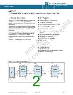
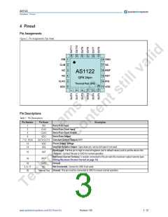
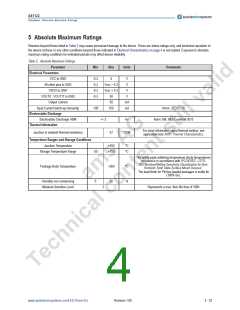
AS1122
Datasheet ꢀ Electrical Characteristics
Timing Characteristics
VDD = +2.7V to +3.6V, TAMB = -40°C to +85ºC. Typical values are at TAMB = +25°C, VDD = 3.3V (unless otherwise specified).
Table 4. Output Timing Characteristics
Symbol
Parameter
Conditions
Min
Typ
Max
Unit
Rise Time OUT1
Fall Time OUT1
tR_OUT
20
ns
20
25
ns
ns
tF_OUT
Average Output Delay Time
(can be turned off on request)
2
tD
1. Value can be factory trimmed for EMI improvement.
2. See Figure 24 on page 10.
Interface Characteristics
VDD = +2.7V to +3.6V, TAMB = -40°C to +85ºC. Typical values are at TAMB = +25°C, VDD = 3.3V (unless otherwise specified).
Table 5. Serial Interface Timing Characteristics
Symbol
fOSC
Parameter
Conditions
Min
8
Typ
Max
12
5
Unit
MHz
MHz
Oscillator Frequency
Data Shift Clock Frequency
10
fCLK
1
1
CLK low time during data shift
CLK low time for data capture
Setup Time
1
ꢁs
ꢁs
ns
ns
ns
ns
ns
ns
ns
ns
tLOW
1
1.5
12
12
2
1.8
2.85
tCAPT
2
SDI, CLKI
tSETUP
2
Hold Time
SDI, CLKI
tHOLD
2
2
Delay CLKI to CLKO3
Delay CLKI to CLKO3
Delay CLKO to SDO3
High Time of CLKO3
Rise Time CLK3
rising CLKI to rising CLKO
rising CLKI to falling CLKO
3.5
103.5
1.5
8
tPD_rising
72
0.8
70
138
3
tPD_falling
2
tPD_SDO
falling edge CLKO
2
100
130
tH_CLKO
CLOAD = 20pF
CLOAD = 20pF
tR_CLK
10
10
tR_DATA
Rise Time Data3
1. See Figure 24 on page 10
2. See Figure 36 on page 16 and Figure 37 on page 16
3. Guaranteed by design and not production tested.
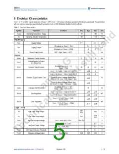
Figure 3. Load Circuit for Digital Output Timing Specifications
200µA
IOL
SDO
CLKO
VDD/2
CLOAD
20pF
200µA
IOH
www.austriamicrosystems.com/LEDꢀDriverꢀICs
Revision 1.00
5 ꢀ 22

 AMSCO [ AMS(艾迈斯) ]