AS1122
Datasheet ꢀ Absolute Maximum Ratings
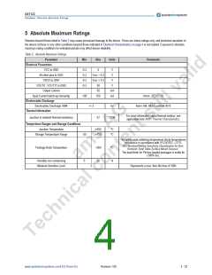
5 Absolute Maximum Ratings
Stresses beyond those listed in Table 2 may cause permanent damage to the device. These are stress ratings only, and functional operation of
the device at these or any other conditions beyond those indicated in Electrical Characteristics on page 4 is not implied. Exposure to absolute
maximum rating conditions for extended periods may affect device reliability.
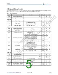
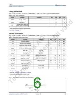
Table 2. Absolute Maximum Ratings
Parameter
Electrical Parameters
Min
Max
Units
Comments
VCC to GND
All other pins to GND
ꢀ0.3
ꢀ0.3
ꢀ0.3
ꢀ0.3
5
VDD + 0.3
VDD + 0.3
30
V
V
VSDO to GND
V
VOUT0 : VOUT11 to GND
Output Current
V
50
mA
mA
Input Current (latchꢀup immunity)
Electrostatic Discharge
Electrostatic Discharge HBM
Thermal Information
ꢀ100
100
Norm: JEDEC 78
+/ꢀ 2
kV
Norm: MIL 883 E method 3015
For more information about thermal metrics, see
application note AN01 Thermal Characteristics.
Junction to ambient thermal resistance
37
°C/W
Temperature Ranges and Storage Conditions
Junction Temperature
+150
+150
ºC
ºC
Storage Temperature Range
ꢀ55
The reflow peak soldering temperature (body temperature)
specified is in accordance with IPC/JEDEC J-STD-
020“Moisture/Reflow Sensitivity Classification for Non-
Hermetic Solid State Surface Mount Devices”.
The lead finish for Pbꢀfree leaded packages is matte tin
(100% Sn).
Package Body Temperature
+260
85
ºC
%
Humidity nonꢀcondensing
Moisture Sensitive Level
5
3
Represents a max. floor life time of 168h
www.austriamicrosystems.com/LEDꢀDriverꢀICs
Revision 1.00
3 ꢀ 22

 AMSCO [ AMS(艾迈斯) ]