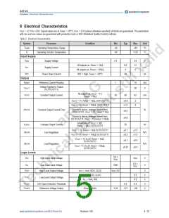
AS1122
Datasheet ꢀ Electrical Characteristics
6 Electrical Characteristics
VDD = +2.7V to +3.6V, Typical values are at TAMB = +25°C, VDD = 3.3V (unless otherwise specified). All limits are guaranteed. The parameters
with min and max values are guaranteed with production tests or SQC (Statistical Quality Control) methods.
Table 3. Electrical Characteristics
Symbol
TAMB
Parameter
Condition
Min
ꢀ40
ꢀ40
Typ
Max
+85
Unit
°C
Operating Temperature Range
Operating Junction Temperature
TJ
+125
°C
Input Supply
VDD
Supply Voltage
Supply Current
2.7
3.6
12
6
V
All outputs on, RIREF = 1kΩ
All outputs on, RIREF = 10kΩ
RST = High, TAMB = +25°C
9.5
4
ICC
mA
nA
IPD
Output
RIREF
Power Down Current
40
Reference Current Resistor
1
10
30
kΩ
Voltage Applied to Output
(OUT0:OUT11)
VOUT
V
All outputs on, VOUT = 1V,
RIREF = 1kΩ
ICOC
Constant Output Current
38
40
42
mA
%
VOUT = 1V, RIREF = 1kΩ, OUT0:OUT11
VOUT = 1V, RIREF = 10kΩ, OUT0:OUT11
±0.8
±1.5
2
4
Device to device, average current from
OUT0:OUT11, VOUT = 1V, RIREF = 1kΩ
∆ICOC
Constant Output Current Error
±0.5
±0.6
20
Device to device, average current from
OUT0:OUT11, VOUT = 1V, RIREF = 10kΩ
All outputs off, VOUT = 30V,
RIREF = 1kΩ, OUT0:OUT11
ILEAK
Leakage Output Current
Line Regulation
nA
VOUT = 1V, RIREF = 1kΩ OUT0:OUT11
VOUT = 1V, RIREF = 10kΩ OUT0:OUT11
±0.1
±0.2
±1.5
±1.5
∆ILNR
%/V
VOUT = 1V to 4V, RIREF = 1kΩ,
±0.1
±0.4
±0.4
OUT0:OUT11
∆ILDR
Load Regulation
%/V
VOUT = 1V to 4V, RIREF = 10kΩ,
±0.01
OUT0:OUT11
Logic Levels
0.8 x
VIH
HighꢀLevel Input Voltage
VDD
V
V
VDD
0.2 x
VDD
VIL
LowꢀLevel Input Voltage
HighꢀLevel Output Voltage
GND
VOH
IOH = ꢀ1mA, SDO, CLKO
IOL = 1mA, SDO, CLKO
IOL = 3mA, IRQ
VDDꢀ0.5
V
V
V
V
V
0.5
0.5
VOL
LowꢀLevel Output Voltage
VLOD
VIREF
LED Open Detection Threshold
Reference Voltage Output
0.3
0.4
RIREF = 1kΩ
1.24
1.27
1.30
www.austriamicrosystems.com/LEDꢀDriverꢀICs
Revision 1.00
4 ꢀ 22

 AMSCO [ AMS(艾迈斯) ]