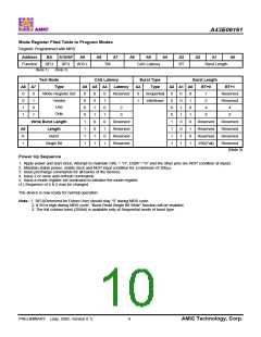
A43E06161
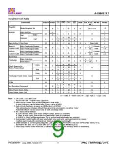
Mode Register Filed Table to Program Modes
Register Programmed with MRS
Address
BA
A10/AP
A9
A8
A7
A6
A5
A4
A3
A2
A1
A0
Function
RFU
RFU
W.B.L
TM
CAS Latency
BT
Burst Length
(Note 1)
(Note 2)
Test Mode
Type
CAS Latency
A6 A5 A4 Latency
Burst Type
Burst Length
A8 A7
A3
Type
A2 A1 A0
BT=0
BT=1
Reserved
Reserved
4
0
0
1
1
0
1
0
1
Mode Register Set
0
0
0
0
1
1
1
1
0
0
1
1
0
0
1
1
0
1
0
1
0
1
0
1
Reserved
-
0
1
Sequential
Interleave
0
0
0
0
1
1
1
1
0
0
1
1
0
0
1
1
0
1
0
1
0
1
0
1
1
2
Vendor
Use
2
4
Only
3
8
8
Reserved
Reserved
Reserved
Reserved
Reserved
Reserved
Reserved
256(Full)
Reserved
Reserved
Reserved
Reserved
Write Burst Length
Length
A9
0
Burst
1
Single Bit
(Note 3)
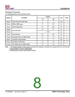
Power Up Sequence
1. Apply power and start clock, Attempt to maintain CKE = “H”, DQM = “H” and the other pins are NOP condition at inputs.
2. Maintain stable power, stable clock and NOP input condition for a minimum of 200µs.
3. Issue precharge commands for all banks of the devices.
4. Issue 2 or more auto-refresh commands.
5. Issue a mode register set command to initialize the mode register.
cf.) Sequence of 4 & 5 may be changed.
The device is now ready for normal operation.
Note : 1. RFU(Reserved for Future Use) should stay “0” during MRS cycle.
2. If A9 is high during MRS cycle, “Burst Read Single Bit Write” function will be enabled.
3. The full column burst (256bit) is available only at Sequential mode of burst type.
PRELIMINARY (July, 2005, Version 0.1)
9
AMIC Technology, Corp.

 AMICC [ AMIC TECHNOLOGY ]