A43E06161
activation of both banks immediately. Also the noise
generated during sensing of each bank of SDRAM is high
requiring some time for power supplies recover before the
other bank can be sensed reliably. tRRD(min) specifies the
minimum time required between activating different banks.
The number of clock cycles required between different bank
activation must be calculated similar to tRCD specification. The
minimum time required for the bank to be active to initiate
sensing and restoring the complete row of dynamic cells is
determined by tRAS(min) specification before a precharge
command to that active bank can be asserted. The maximum
time any bank can be in the active state is determined by
tRAS(max). The number of cycles for both tRAS(min) and
tRAS(max) can be calculated similar to tRCD specification.
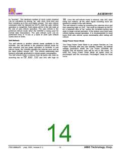
DQM and zero cycle for write, which means DQM masking
occurs two cycles later in the read cycle and occurs in the
same cycle during write cycle. DQM operation is
synchronous with the clock, therefore the masking occurs for
a complete cycle. The DQM signal is important during burst
interrupts of write with read or precharge in the SDRAM. Due
to asynchronous nature of the internal write, the DQM
operation is critical to avoid unwanted or incomplete writes
when the complete burst write is not required.
Precharge
The precharge operation is performed on an active bank by
asserting low on
,
,
and A10/AP with valid BA
WE
CS RAS
of the bank to be precharged. The precharge command can
be asserted anytime after tRAS(min) is satisfied from the bank
activate command in the desired bank. “tRP” is defined as the
minimum time required to precharge a bank.
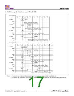
Burst Read
The burst read command is used to access burst of data on
consecutive clock cycles from an active row in an active
bank. The burst read command is issued by asserting low on
The minimum number of clock cycles required to complete
row precharge is calculated by dividing “tRP” with clock cycle
time and rounding up to the next higher integer. Care should
be taken to make sure that burst write is completed or DQM
is used to inhibit writing before precharge command is
asserted. The maximum time any bank can be active is
specified by tRAS(max). Therefore, each bank has to be
precharged within tRAS(max) from the bank activate
command. At the end of precharge, the bank enters the idle
state and is ready to be activated again.
and
with
being high on the positive edge of
WE
CS
CAS
the clock. The bank must be active for at least tRCD(min)
before the burst read command is issued. The first output
appears CAS latency number of clock cycles after the issue
of burst read command. The burst length, burst sequence
and latency from the burst read command is determined by
the mode register which is already programmed. The burst
read can be initiated on any column address of the active
row. The address wraps around if the initial address does not
start from a boundary such that number of outputs from each
I/O are equal to the burst length programmed in the mode
register. The output goes into high-impedance at the end of
the burst, unless a new burst read was initiated to keep the
data output gapless. The burst read can be terminated by
issuing another burst read or burst write in the same bank or
the other active bank or a precharge command to the same
bank. The burst stop command is valid at every page burst
length.
Entry to Power Down, Auto refresh, Self refresh and Mode
register Set etc, is possible only when both banks are in idle
state.
Auto Precharge
The precharge operation can also be performed by using
auto precharge. The SDRAM internally generates the timing
to satisfy tRAS(min) and “tRP” for the programmed burst length
and CAS latency. The auto precharge command is issued at
the same time as burst read or burst write by asserting high
on A10/AP. If burst read or burst write command is issued
with low on A10/AP, the bank is left active until a new
command is asserted. Once auto precharge command is
given, no new commands are possible to that particular bank
until the bank achieves idle state.
Burst Write
The burst write command is similar to burst read command,
and is used to write data into the SDRAM consecutive clock
cycles in adjacent addresses depending on burst length and
burst sequence. By asserting low on
,
and
with
WE
CS CAS
Both Banks Precharge
valid column address, a write burst is initiated. The data
inputs are provided for the initial address in the same clock
cycle as the burst write command. The input buffer is
deselected at the end of the burst length, even though the
internal writing may not have been completed yet. The writing
can not complete to burst length. The burst write can be
terminated by issuing a burst read and DQM for blocking
data inputs or burst write in the same or the other active
bank. The burst stop command is valid only at full page burst
length where the writing continues at the end of burst and the
burst is wrap around. The write burst can also be terminated
by using DQM for blocking data and precharging the bank
“tRDL” after the last data input to be written into the active row.
See DQM OPERATION also.
Both banks can be precharged at the same time by using
Precharge all command. Asserting low on
,
and
CS RAS
with high on A10/AP after both banks have satisfied
WE
tRAS(min) requirement, performs precharge on both banks. At
the end of tRP after performing precharge all, both banks are
in idle state.
Auto Refresh
The storage cells of SDRAM need to be refreshed every
32ms to maintain data. An auto refresh cycle accomplishes
refresh of a single row of storage cells. The internal counter
increments automatically on every auto refresh cycle to
refresh all the rows. An auto refresh command is issued by
DQM Operation
asserting low on
,
and
with high on CKE and
CAS
CS RAS
The DQM is used to mask input and output operation. It
. The auto refresh command can only be asserted with
WE
both banks being in idle state and the device is not in power
down mode (CKE is high in the previous cycle). The time
required to complete the auto refresh operation is specified
works similar to
during read operation and inhibits writing
OE
during write operation. The read latency is two cycles from
PRELIMINARY (July, 2005, Version 0.1)
12
AMIC Technology, Corp.

 AMICC [ AMIC TECHNOLOGY ]