PI6049A Data Sheet
__________________________________________________________________________________________
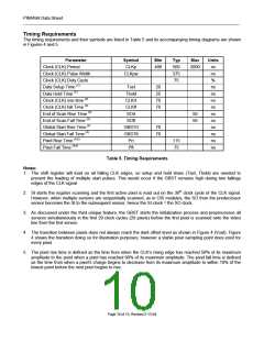
Timing Requirements
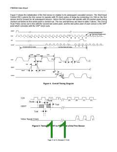
The timing requirements and their symbols are listed in Table 5 and its accompanying timing diagrams are shown
in Figures 4 and 5.
Parameter
Clock (CLK) Period
Symbol
CLKp
CLKpw
Min
400
Typ
500
375
75
Max
2000
Units
ns
ns
%
Clock (CLK) Pulse Width
Clock (CLK) Duty Cycle
Data Setup Time (1)
Tset
Thold
CLKrt
CLKft
SOrt
20
25
70
70
ns
ns
ns
ns
ns
ns
ns
ns
ns
ns
Data Hold Time (1)
Clock (CLK) rise time (2)
Clock (CLK) fall Time (2)
End of Scan Rise Time (2)
End of Scan Fall Time (2)
Global Start Rise Time (3)
Global Start Fall Time (3)
Pixel Rise Time (4,5)
50
50
SOft
GBSTrt
GBSTft
Prt
70
70
115
75
Pixel Fall Time (4,5)
Pft
Table 5. Timing Requirements
Notes:
1. The shift register will load on all falling CLK edges, so setup and hold times (Tset, Thold) are needed to
prevent the loading of multiple start pulses. This would occur if the GBST remains high during two fallings
edges of the CLK signal.
2. SI starts the register scanning and the first active pixel is read out on the 30th clock cycle of the CLK signal.
However, when multiple sensors are sequentially scanned, as in CIS modules, the SO from the predecessor
sensor becomes the SI to the subsequent sensor, hence the SI clock = the SO clock.
3. As discussed under the third unique feature, the GBST starts the initialization process and preprocesses all
sensors simultaneously in the first 29 clock cycles (29 pixels) before the first pixel is scanned onto the video
line from the first sensor.
4. The transition between pixels does not always reach the dark offset level as shown in Figure 4 (Vout). Figure
4 shows the transition doing so for illustration purposes; however a stable pixel sampling point does exist for
every pixel.
5. The pixel rise time is defined as the time from when the CLK’s rising edge has reached 50% of its maximum
amplitude to the point when a pixel has reached 90% of its maximum amplitude. The pixel fall time is defined
as the time from when a pixel’s charge begins to decrease from its maximum amplitude to within 10% of the
lowest point before the next pixel begins to rise.
Page 10 of 13, Revised 2-13-04

 AMI [ AMI SEMICONDUCTOR ]