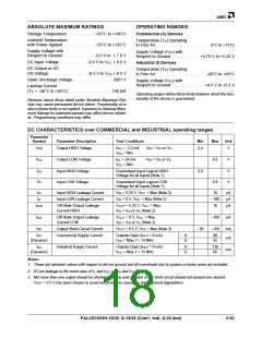
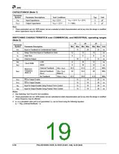
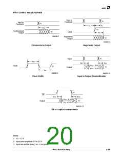
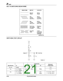
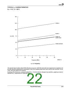
AMD
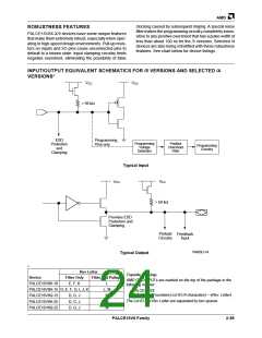
clocking caused by subsequent ringing. A special noise
filtermakestheprogrammingcircuitrycompletelyinsen-
sitive to any positive overshoot that has a pulse width of
less than about 100 ns for the /5 versions. Selected /4
devices are also being retrofitted with these robustness
features. See chart below for device listings.
ROBUSTNESS FEATURES
PALCE16V8X-X/5 devices have some unique features
that make them extremely robust, especially when oper-
ating in high-speed design environments. Pull-up resis-
tors on inputs and I/O pins cause unconnected pins to
default to a known state. Input clamping circuitry limits
negative overshoot, eliminating the possibility of false
INPUT/OUTPUT EQUIVALENT SCHEMATICS FOR /5 VERSIONS AND SELECTED /4
VERSIONS*
VCC
VCC
> 50 kΩ
ESD
Protection
and
Programming
Pins only
Programming
Voltage
Detection
Positive
Overshoot
Filter
Programming
Circuitry
Clamping
Typical Input
VCC
VCC
> 50 kΩ
Provides ESD
Protection and
Clamping
Preload Feedback
Circuitry
Input
16493D-14
Typical Output
*
Rev Letter
Topside Marking:
Device
PALCE16V8H-10
PALCE16V8H-15 D, E, F, G, I, J, K
Filter Only
Filter and Pullups
AMD CMOS PLD’s are marked on the top of the package in the
following manner:
E, F, K
L
L, M
M
PALCEXXXX
Date Code (3 numbers) Lot ID (4 characters)– –(Rev. Letter)
PALCE16V8Q-15
PALCE16V8H-25
PALCE16V8Q-25
D, G, J
D, G, J
D, G, J
The Lot ID and Rev Letter are separated by two spaces.
M
M
PALCE16V8 Family
2-59

 AMD [ AMD ]