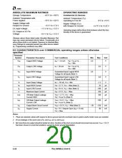
AMD
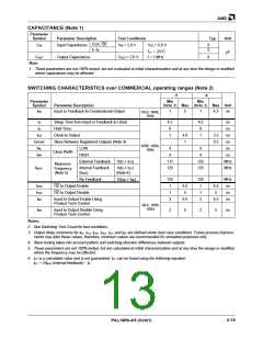
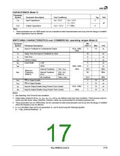
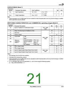
CAPACITANCE (Note 1)
Parameter
Symbol
Parameter Description
Test Conditions
Typ
Unit
CIN
Input Capacitance
VIN = 2.0 V
VCC = 5.0 V
TA = 25°C
f = 1 MHz
5
8
pF
COUT
Output Capacitance
VOUT = 2.0 V
Note:
1. These parameters are not 100% tested, but are evaluated at initial characterization and at any time the design is modified
where capacitance may be affected.
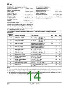
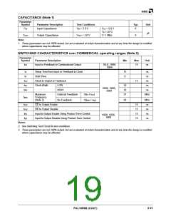
SWITCHING CHARACTERISTICS over COMMERCIAL operating ranges (Note 2)
Parameter
Symbol
Min
(Note 3)
Parameter Description
Max
Unit
tPD
Input or Feedback to Combinatorial Output
16L8, 16R6,
16R4
3
10
ns
tS
tH
Setup Time from Input or Feedback to Clock
Hold Time
10
0
ns
ns
tCO
tWL
tWH
Clock to Output
3
7
ns
Clock Width
LOW
8
ns
HIGH
16R8, 16R6,
16R4
8
ns
External Feedback
1/(tS + tCO
)
58.8
60
MHz
MHz
Maximum
Frequency
(Note 4)
fMAX
Internal Feedback
1/(tS + tCF
(Note 5)
)
(fCNT
)
No Feedback
1/(tWH + tWL
)
62.5
MHz
ns
tPZX
tPXZ
OE to Output Enable
OE to Output Disable
2
2
3
3
10
10
10
10
ns
tEA
Input to Output Enable Using Product Term Control
Input to Output Disable Using Product Term Control
16L8, 16R6,
16R4
ns
tER
ns
Notes:
2. See Switching Test Circuit for test conditions.
3. Output delay minimums for tPD, tCO, tPZX, tPXZ, tEA, and tER are defined under best case conditions. Future process improve-
ments may alter these values; therefore, minimum values are recommended for simulation purposes only.
4. These parameters are not 100% tested, but are calculated at initial characterization and at any time the design is modified
where the frequency may be affected.
5. tCF is a calculated value and is not guaranteed. tCF can be found using the following equation:
tCF = 1/fMAX (internal feedback) – tS.
2-19
PAL16R8D/2 (Com’l)

 AMD [ AMD ]