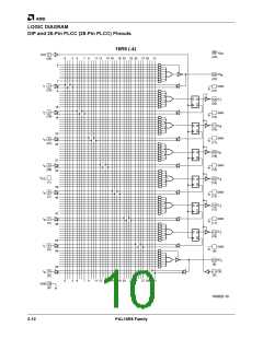
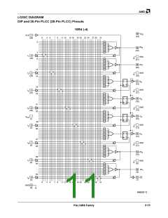
AMD
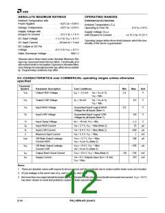
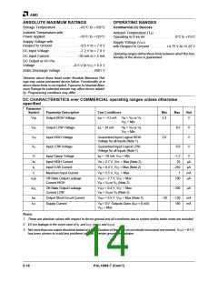
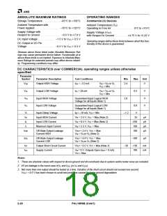
ABSOLUTE MAXIMUM RATINGS
OPERATING RANGES
Storage Temperature . . . . . . . . . . . –65°C to +150°C
Commercial (C) Devices
Ambient Temperature with
Ambient Temperature (TA)
Power Applied . . . . . . . . . . . . . . . . . –55°C to +125°C
Operating in Free Air . . . . . . . . . . . . . . 0°C to +75°C
Supply Voltage with
Respect to Ground . . . . . . . . . . . . . –0.5 V to + 7.0 V
Supply Voltage (VCC
with Respect to Ground . . . . . . . . +4.75 V to +5.25 V
)
DC Input Voltage . . . . . . . . . . . . . . . –1.2 V to + 7.0 V
DC Input Current . . . . . . . . . . . . . . –30 mA to + 5 mA
Operating ranges define those limits between which the func-
tionality of the device is guaranteed.
DC Output or I/O Pin
Voltage . . . . . . . . . . . . . . . . . . –0.5 V to VCC + 0.5 V
Static Discharge Voltage . . . . . . . . . . . . . . . . . 2001 V
Stresses above those listed under Absolute Maximum Rat-
ings may cause permanent device failure. Functionality at or
above these limits is not implied. Exposure to Absolute Maxi-
mum Ratings for extended periods may affect device reliabil-
ity. Programming conditions may differ.
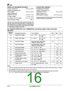
DC CHARACTERISTICS over COMMERCIAL operating ranges unless otherwise
specified
Parameter
Symbol
Parameter Description
Test Conditions
Min
Max
Unit
VOH
Output HIGH Voltage
IOH = –3.2 mA
VIN = VIH or VIL
CC = Min
2.4
V
V
VOL
VIH
VIL
Output LOW Voltage
Input HIGH Voltage
Input LOW Voltage
IOL = 24 mA
VIN = VIH or VIL
CC = Min
0.5
V
V
V
V
Guaranteed Input Logical HIGH
Voltage for all Inputs (Note 1)
2.0
Guaranteed Input Logical LOW
Voltage for all Inputs (Note 1)
0.8
VI
IIH
IIL
Input Clamp Voltage
Input HIGH Current
Input LOW Current
Maximum Input Current
IIN = –18 mA, VCC = Min
–1.2
25
V
VIN = 2.7 V, VCC = Max (Note 2)
VIN = 0.4 V, VCC = Max (Note 2)
VIN = 5.5 V, VCC = Max
µA
µA
mA
µA
–250
1
II
IOZH
Off-State Output Leakage
Current HIGH
VOUT = 2.7 V, VCC = Max
VIN = VIH or VIL (Note 2)
100
IOZL
Off-State Output Leakage
Current LOW
VOUT = 0.4 V, VCC = Max
–100
µA
VIN = VIH or VIL (Note 2)
ISC
ICC
Output Short-Circuit Current
Supply Current
VOUT = 0.5 V, VCC = Max (Note 3)
–30
–130
180
mA
mA
VIN = 0 V, Outputs Open (IOUT = 0 mA)
VCC = Max
Notes:
1. These are absolute values with respect to device ground and all overshoots due to system and/or tester noise are included.
2. I/O pin leakage is the worst case of IIL and IOZL (or IIH and IOZH).
3. Not more than one output should be tested at a time. Duration of the short-circuit should not exceed one second. VOUT = 0.5 V
has been chosen to avoid test problems caused by tester ground degradation.
2-16
PAL16R8-7 (Com’l)

 AMD [ AMD ]