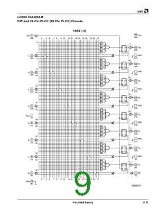
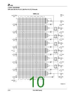
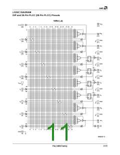
AMD
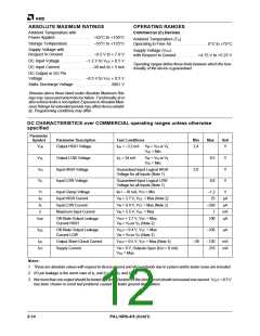
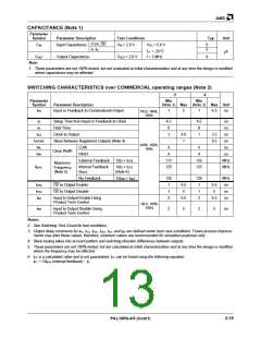
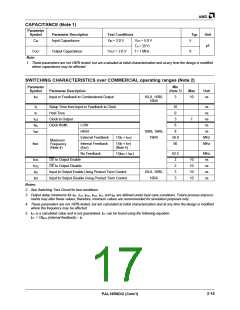
CAPACITANCE (Note 1)
Parameter
Symbol
Parameter Description
Test Conditions
Typ
Unit
CLK, OE
CIN
Input Capacitance
VIN = 2.0 V
VCC = 5.0 V
8
I1–I8
5
TA = 25°C
pF
COUT
Output Capacitance
VOUT = 2.0 V
f = 1 MHz
8
Note:
1. These parameters are not 100% tested, but are evaluated at initial characterization and at any time the design is modified
where capacitance may be affected.
SWITCHING CHARACTERISTICS over COMMERCIAL operating ranges (Note 2)
-5
-4
Parameter
Symbol
Min
Min
Parameter Description
(Note 3) Max (Note 3) Max Unit
tPD
Input or Feedback to Combinatorial Output
1
5
1
4.5
ns
16L8, 16R8,
16R4
tS
tH
Setup Time from Input or Feedback to Clock
Hold Time
4.5
0
4.5
0
ns
ns
tCO
Clock to Output
1
4.0
1
1
3.5
0.5
ns
tSKEWR
tWL
Skew Between Registered Outputs (Note 4)
ns
16R8, 16R6,
16R4
LOW
Clock Width
HIGH
4
4
ns
tWH
4
4
ns
External Feedback
Internal Feedback
1/(tS + tCO
)
117
125
125
125
MHz
MHz
Maximum
Frequency
(Note 5)
fMAX
1/(tS + tCF
(Note 6)
)
(fCNT
)
No Feedback
1/(tWH + tWL
)
125
1
125
1
MHz
ns
tPZX
tPXZ
tEA
OE to Output Enable
OE to Output Disable
6.5
5
6.5
5
1
1
ns
Input to Output Enable Using
Product Term Control
2
6.5
2
6.5
ns
16L8, 16R6,
16R4
tER
Input to Output Disable Using
Product Term Control
2
5
2
5
ns
Notes:
2. See Switching Test Circuit for test conditions.
3. Output delay minimums for tPD, tCO, tPZX, tPXZ, tEA, and tER are defined under best case conditions. Future process improve-
ments may alter these values; therefore, minimum values are recommended for simulation purposes only.
4. Skew testing takes into account pattern and switching direction differences between outputs.
5. These parameters are not 100% tested, but are calculated at initial characterization and at any time the design is modified
where the frequency may be affected.
6. tCF is a calculated value and is not guaranteed. tCF can be found using the following equation:
tCF = 1/fMAX (internal feedback) – tS.
2-15
PAL16R8-4/5 (Com’l)

 AMD [ AMD ]