F
PARAMETERS
MAX
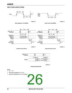
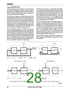
The parameter f
the device is guaranteed to operate. Because the flexi-
bility inherent in programmable logic devices offers a
is the maximum clock rate at which
The third type of design is a simple data path applica-
tion. In this case, input data is presented to the flip-flop
and clocked through; no feedback is employed. Under
these conditions, the period is limited by the sum of the
MAX
choice of clocked flip-flop designs, f
is specified for
MAX
three types of synchronous designs.
data setup time and the data hold time (t + t ). How-
S
H
ever, a lower limit for the period of each f
type is the
MAX
The first type of design is a state machine with feed-
back signals sent off-chip.This external feedback could
go back to the device inputs, or to a second device in a
multi-chip state machine.The slowest path defining the
period is the sum of the clock-to-output time and the
minimum clock period (t
+ t ). Usually, this mini-
WH
WL
mum clock period determines the period for the third
, designated “f no feedback.”
f
MAX
MAX
For devices with input registers, one additional f
pa-
MAX
input setup time for the external signals (t + t ). The
rameter is specified: f
. Because this involves no
S
CO
MAXIR
reciprocal, f
, is the maximum frequency with exter-
feedback, it is calculated the same way as f
no
MAX
MAX
nal feedback or in conjunction with an equivalent speed
device. This f is designated “f external.”
feedback. The minimum period will be limited either by
the sum of the setup and hold times (t
+ t ) or the
MAX
MAX
SIR
HIR
sum of the clock widths (t
+ t
). The clock
WICL
WICH
The second type of design is a single-chip state ma-
chine with internal feedback only. In this case, flip-flop
inputs are defined by the device inputs and flip-flop out-
puts. Under these conditions, the period is limited by
the internal delay from the flip-flop outputs through the
internal feedback and logic to the flip-flop inputs. This
widths are normally the limiting parameters, so that
is specified as 1/(t + t ). Note that if both
f
MAXIR
WICL
WICH
input and output registers are use in the same path, the
overall frequency will be limited by t
.
ICS
All frequencies except f
internal are calculated from
MAX
f
is designated “f
internal”. A simple internal
other measured AC parameters. f
internal is mea-
MAX
MAX
MAX
counter is a good example of this type of design; there-
sured directly.
fore, this parameter is sometimes called “f
”
CNT.
CLK
CLK
(SECOND
CHIP)
REGISTER
LOGIC
REGISTER
LOGIC
t
t
t
S
S
CO
f
External; 1/(t + t
)
f
Internal (f
)
MAX
S
CO
MAX
CNT
CLK
CLK
REGISTER
LOGIC
REGISTER
LOGIC
t
S
t
t
HIR
SIR
f
No Feedback; 1/(t + t ) or 1/(t
+ t
)
f
; 1/(t
+ t ) or 1/(t
+ t
)
MAX
S
H
WH
WL
MAXIR
SIR
HIR
WICL
WICH
20405B-21
28
MACH211SP-7/10/12/15/20

 AMD [ AMD ]