P R E L I M I N A R Y
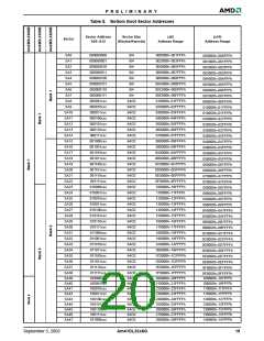
An erase operation can erase one sector, multiple sec-
Word/Byte Configuration
tors, or the entire device. Tables 6–8 indicate the
address space that each sector occupies. The device
address space is divided into two banks: Bank 1 con-
tains the boot/parameter sectors, and Bank 2 contains
the larger, code sectors of uniform size. A “bank ad-
dress” is the address bits required to uniquely select a
bank. Similarly, a “sector address” is the address bits
required to uniquely select a sector.
The CIOf pin controls whether the device data I/O pins
operate in the byte or word configuration. If the CIOf
pin is set at logic ‘1’, the device is in word configura-
tion, DQ15–DQ0 are active and controlled by CE# and
OE#.
If the CIOf pin is set at logic ‘0’, the device is in byte
configuration, and only data I/O pins DQ7–DQ0 are
active and controlled by CE# and OE#. The data I/O
pins DQ14–DQ8 are tri-stated, and the DQ15 pin is
used as an input for the LSB (A-1) address function.
I
CC2 in the DC Characteristics table represents the ac-
tive current specification for the write mode. The AC
Characteristics section contains timing specification
tables and timing diagrams for write operations.
Requirements for Reading Array Data
To read array data from the outputs, the system must
drive the CE#f and OE# pins to VIL. CE#f is the power
control and selects the device. OE# is the output con-
trol and gates array data to the output pins. WE#
should remain at VIH. The CIOf pin determines
whether the device outputs array data in words or
bytes.
Accelerated Program Operation
The device offers accelerated program operations
through the ACC function. This is one of two functions
provided by the WP#/ACC pin. This function is prima-
rily intended to allow faster manufacturing throughput
at the factory.
If the system asserts VHH on this pin, the device auto-
matically enters the aforementioned Unlock Bypass
mode, temporarily unprotects any protected sectors,
and uses the higher voltage on the pin to reduce the
time required for program operations. The system
would use a two-cycle program command sequence
as required by the Unlock Bypass mode. Removing
The internal state machine is set for reading array data
upon device power-up, or after a hardware reset. This
ensures that no spurious alteration of the memory
content occurs during the power transition. No com-
mand is necessary in this mode to obtain array data.
Standard microprocessor read cycles that assert valid
addresses on the device address inputs produce valid
data on the device data outputs. Each bank remains
enabled for read access until the command register
contents are altered.
V
HH from the WP#/ACC pin returns the device to nor-
mal operation. Note that the WP#/ACC pin must not
be at VHH for operations other than accelerated pro-
gramming, or device damage may result. In addition,
the WP#/ACC pin must not be left floating or uncon-
nected; inconsistent behavior of the device may result.
See “Requirements for Reading Array Data” for more
information. Refer to the AC Flash Read-Only Opera-
tions table for timing specifications and to Figure 14 for
the timing diagram. ICC1 in the DC Characteristics
table represents the active current specification for
reading array data.
Autoselect Functions
If the system writes the autoselect command se-
quence, the device enters the autoselect mode. The
system can then read autoselect codes from the inter-
nal register (which is separate from the memory array)
on DQ7–DQ0. Standard read cycle timings apply in
this mode. Refer to the Autoselect Mode and Autose-
lect Command Sequence sections for more
information.
Writing Commands/Command Sequences
To write a command or command sequence (which in-
cludes programming data to the device and erasing
sectors of memory), the system must drive WE# and
CE#f to VIL, and OE# to VIH.
For program operations, the CIOf pin determines
whether the device accepts program data in bytes or
words. Refer to “Word/Byte Configuration” for more
information.
Simultaneous Read/Write Operations with
Zero Latency
This device is capable of reading data from one bank
of memory while programming or erasing in the other
bank of memory. An erase operation may also be sus-
pended to read from or program to another location
within the same bank (except the sector being
erased). Figure 21 shows how read and write cycles
may be initiated for simultaneous operation with zero
latency. ICC6 and ICC7 in the DC Characteristics table
represent the current specifications for read-while-pro-
gram and read-while-erase, respectively.
The device features an Unlock Bypass mode to facil-
itate faster programming. Once a bank enters the
Unlock Bypass mode, only two write cycles are re-
quired to program a word or byte, instead of four. The
“Word/Byte Configuration” section has details on pro-
gramming data to the device using both standard and
Unlock Bypass command sequences.
September 5, 2002
Am41DL32x8G
15

 AMD [ AMD ]