P R E L I M I N A R Y
RESET# pin is driven low for at least a period of tRP
,
Standby Mode
the device immediately terminates any operation in
progress, tristates all output pins, and ignores all
read/write commands for the duration of the RESET#
pulse. The device also resets the internal state ma-
chine to reading array data. The operation that was
interrupted should be reinitiated once the device is
ready to accept another command sequence, to en-
sure data integrity.
When the system is not reading or writing to the de-
vice, it can place the device in the standby mode. In
this mode, current consumption is greatly reduced,
and the outputs are placed in the high impedance
state, independent of the OE# input.
The device enters the CMOS standby mode when the
CE#f and RESET# pins are both held at VCC ± 0.3 V.
(Note that this is a more restricted voltage range than
VIH.) If CE#f and RESET# are held at VIH, but not
within VCC ± 0.3 V, the device will be in the standby
mode, but the standby current will be greater. The de-
vice requires standard access time (tCE) for read
access when the device is in either of these standby
modes, before it is ready to read data.
Current is reduced for the duration of the RESET#
pulse. When RESET# is held at VSS ± 0.3 V, the de-
vice draws CMOS standby current (ICC4). If RESET# is
held at VIL but not within VSS ± 0.3 V, the standby cur-
rent will be greater.
The RESET# pin may be tied to the system reset cir-
cuitry. A system reset would thus also reset the Flash
memory, enabling the system to read the boot-up firm-
ware from the Flash memory.
If the device is deselected during erasure or program-
ming, the device draws active current until the
operation is completed.
If RESET# is asserted during a program or erase op-
eration, the RY/BY# pin remains a “0” (busy) until the
internal reset operation is complete, which requires a
time of tREADY (during Embedded Algorithms). The
system can thus monitor RY/BY# to determine
whether the reset operation is complete. If RESET# is
asserted when a program or erase operation is not ex-
ecuting (RY/BY# pin is “1”), the reset operation is
completed within a time of tREADY (not during Embed-
ded Algorithms). The system can read data tRH after
the RESET# pin returns to VIH.
ICC3 in the DC Characteristics table represents the
standby current specification.
Automatic Sleep Mode
The automatic sleep mode minimizes Flash device en-
ergy consumption. The device automatically enables
this mode when addresses remain stable for tACC
+
30 ns. The automatic sleep mode is independent of
the CE#f, WE#, and OE# control signals. Standard ad-
dress access timings provide new data when
addresses are changed. While in sleep mode, output
data is latched and always available to the system.
ICC4 in the DC Characteristics table represents the
automatic sleep mode current specification.
Refer to the AC Characteristics tables for RESET# pa-
rameters and to Figure 15 for the timing diagram.
Output Disable Mode
RESET#: Hardware Reset Pin
The RESET# pin provides a hardware method of re-
setting the device to reading array data. When the
When the OE# input is at VIH, output from the device is
disabled. The output pins are placed in the high
impedance state.
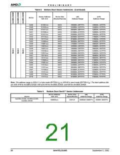
Table 5. Device Bank Division
Bank 1
Device
Bank 2
Sector Sizes
Part Number
Megabits
Sector Sizes
Megabits
Eight 8 Kbyte/4 Kword,
seven 64 Kbyte/32 Kword
Fifty-six
64 Kbyte/32 Kword
Am29DL322G
Am29DL323G
Am29DL324G
4 Mbit
28 Mbit
Eight 8 Kbyte/4 Kword,
fifteen 64 Kbyte/32 Kword
Forty-eight
64 Kbyte/32 Kword
8 Mbit
24 Mbit
16 Mbit
Eight 8 Kbyte/4 Kword,
thirty-one 64 Kbyte/32 Kword
Thirty-two
64 Kbyte/32 Kword
16 Mbit
16
Am41DL32x8G
September 5, 2002

 AMD [ AMD ]